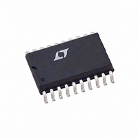
LTC1609CSW#TRPBF Linear Technology, LTC1609CSW#TRPBF Datasheet

LTC1609CSW#TRPBF
Specifications of LTC1609CSW#TRPBF
Available stocks
Related parts for LTC1609CSW#TRPBF
LTC1609CSW#TRPBF Summary of contents
Page 1
... A separate convert start input (R/C) and a data ready signal (BUSY) ease connections to FIFOs, DSPs and microprocessors. , LTC and LT are registered trademarks of Linear Technology Corporation DIG + ...
Page 2
LTC1609 ABSOLUTE MAXIMUM V .......................................................................... 7V ANA ........................................................... 0.3V DIG ANA V ........................................................................... 7V DIG Ground Voltage Difference DGND, AGND1 and AGND2 .............................. 0.3V Analog Inputs (Note ................................................ ...
Page 3
U CONVERTER CHARACTERISTICS temperature range, otherwise specifications are at T PARAMETER CONDITIONS Bipolar Zero Error Drift Bipolar Ranges Unipolar Zero Error External Reference = 2.5V, Unipolar Ranges Unipolar Zero Error Drift Unipolar Ranges Full-Scale Error Drift Full-Scale Error External Reference ...
Page 4
LTC1609 U U DIGITAL I PUTS A D DIGITAL OUTPUTS operating temperature range, otherwise specifications are at T SYMBOL PARAMETER V High Level Input Voltage IH V Low Level Input Voltage IL I Digital Input Current IN C Digital Input ...
Page 5
W U POWER REQUIREMENTS otherwise specifications are (Note 5) A SYMBOL PARAMETER V Positive Supply Voltage DD I Positive Supply Current DD P Power Dissipation DIS Note 1: Absolute Maximum Ratings are those values beyond ...
Page 6
LTC1609 W U TYPICAL PERFOR A CE CHARACTERISTICS Supply Current vs Supply Voltage 15 200kHz SAMPLE 14.5 14.0 13.5 13.0 12.5 12.0 11.5 11.0 4.5 5.0 5.5 4.75 5.25 SUPPLY VOLTAGE (V) 1609 G01 Typical INL Curve 2.0 ...
Page 7
PIN FUNCTIONS (20-Pin SO/28-Pin SSOP) R1 (Pin 1/Pin 1): Analog Input. See Table 1 and Figure 1 IN for input range connections. AGND1 (Pin 2/Pin 2): Analog Ground. Tie to analog ground plane. R2 (Pin 3/Pin 3): ...
Page 8
LTC1609 U U FUNCTIONAL BLOCK DIAGRA 20k R1 IN 10k 20k REF 2.5V REF REF BUF CAP (2.5V) AGND1 AGND2 INTERNAL DGND CLOCK U U APPLICATIO S I FOR ATIO Conversion Details The LTC1609 ...
Page 9
... In the unipolar case, the data is in straight binary format (SB/BTC = HIGH). Figures 4a and 4b show the transfer characteristics of the LTC1609. LinearView is a trademark of Linear Technology Corporation. LTC1609 , R2 and R3 ...
Page 10
LTC1609 U U APPLICATIO S I FOR ATIO INPUT RANGE WITHOUT TRIM 200 10V 33.2k + 2.2 F 200 33. 2.2 F Figure 3a. Offset/Gain ...
Page 11
U U APPLICATIO S I FOR ATIO INPUT RANGE WITHOUT TRIM V 100 10V 33.2k + 2.2 F 200 V 5V 33. 100 3.3V 33.2k + 2.2 F Table 1b. Analog Input Range Connections for ...
Page 12
LTC1609 U U APPLICATIO S I FOR ATIO Table 1c. LTC1609 Output Codes for Ideal Input Voltages DESCRIPTION Full-Scale Range 10V 5V Least Significant Bit 305 V 153 V +Full Scale (FS – 1LSB) 9.999695V 4.999847V 3.339898V Midscale 0V 0V ...
Page 13
U U APPLICATIO S I FOR ATIO Dynamic Performance FFT (Fast Fourier Transform) test techniques are used to test the ADC’s frequency response, distortion and noise at the rated throughput. By applying a low distortion sine wave and analyzing the ...
Page 14
LTC1609 U U APPLICATIO S I FOR ATIO Power Shutdown When the PWRD pin is tied high, power consumption drops to a typical value from a specified maxi- mum of 100mW. In the power shutdown mode, the ...
Page 15
U U APPLICATIO S I FOR ATIO External Clock Mode With the EXT/INT pin tied high, the DATACLK pin becomes a digital input and the LTC1609 can accept an externally supplied data clock. There are several ways in which the ...
Page 16
LTC1609 U U APPLICATIO S I FOR ATIO External Data Clock Data Read After the Conversion Figure 10 shows how the result from the current conver- sion can be read out after the conversion has been com- pleted. The externally ...
Page 17
U U APPLICATIO S I FOR ATIO EXTERNAL DATACLK BUSY t 17 SYNC DATA Figure 11. Conversion and Read Timing Using a Discontinuous Data Clock (EXT/INT Tied High, CS Tied ...
Page 18
LTC1609 U U APPLICATIO S I FOR ATIO 0 EXTERNAL DATACLK R BUSY SYNC DATA TAG Figure 12. Conversion and Read Timing Using an External Data Clock (EXT/INT Tied High). Read Previous Conversion Result During ...
Page 19
U U APPLICATIO S I FOR ATIO R/C BUSY DCLK DATA B15 B14 B13 B12 B11 B10 OUT Figure 14. Data Output from Cascading Two (CS = Low, TAG (#2) = Low) LTC1609s Together Output Data ...
Page 20
LTC1609 U U APPLICATIO S I FOR ATIO R4 200 E15 R4 R5 100 E16 33k E17 R6 5V JP1 Figure 15a. LTC1609 “Postage Stamp” Evaluation Circuit Schematic ...
Page 21
U U APPLICATIO S I FOR ATIO Figure 15b. LTC1609 “Postage Stamp” Evaluation Board Silkscreen (2 Actual Size) Figure 15d. LTC1609 “Postage Stamp” Evaluation Board Bottom Metal Layer (2 Actual Size Figure 15c. LTC1609 “Postage Stamp” Evaluation Board ...
Page 22
LTC1609 U U APPLICATIO S I FOR ATIO 200 33. 10V OFFSET LTC1662 TRIM CS/LD CS/LD V OUTA SCK SCK GND GAIN SDI SDI V CC TRIM 5V REF V OUTB + 2.2 F 0.1 F 200 0V ...
Page 23
... FLASH SHALL NOT EXCEED .254mm (.010") PER SIDE Information furnished by Linear Technology Corporation is believed to be accurate and reliable. However, no responsibility is assumed for its use. Linear Technology Corporation makes no represen- tation that the interconnection of its circuits as described herein will not infringe on existing patent rights. ...
Page 24
... Low Glitch Settling Time, Serial I/O SO-8 Package, Micropower, Serial I/O www.linear.com 0.394 – 0.419 (10.007 – 10.643 0.037 – 0.045 (0.940 – 1.143) 0.004 – 0.012 (0.102 – 0.305) S20 (WIDE) 1098 LT/TP 0302 1.5K REV A • PRINTED IN THE USA LINEAR TECHNOLOGY CORPORATION 2000 1609fa ...


