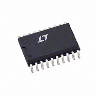
LTC1609CSW#TRPBF Linear Technology, LTC1609CSW#TRPBF Datasheet - Page 7

LTC1609CSW#TRPBF
Manufacturer Part Number
LTC1609CSW#TRPBF
Description
IC ADC SRL 16BIT 200KSPS 20-SOIC
Manufacturer
Linear Technology
Datasheet
1.LTC1609CSW.pdf
(24 pages)
Specifications of LTC1609CSW#TRPBF
Number Of Bits
16
Sampling Rate (per Second)
200k
Data Interface
Serial
Number Of Converters
1
Power Dissipation (max)
100mW
Voltage Supply Source
Analog and Digital
Operating Temperature
0°C ~ 70°C
Mounting Type
Surface Mount
Package / Case
20-SOIC (0.300", 7.50mm Width)
Lead Free Status / RoHS Status
Lead free / RoHS Compliant
Available stocks
Company
Part Number
Manufacturer
Quantity
Price
PIN
R1
for input range connections.
AGND1 (Pin 2/Pin 2): Analog Ground. Tie to analog ground
plane.
R2
for input range connections.
R3
for input range connections.
NC (28-Pin SSOP Only—Pins 5, 8, 10, 11, 18, 20, 22,
23): No Connect.
CAP (Pin 5/Pin 6): Reference Buffer Output. Bypass with
2.2 F tantalum capacitor.
REF (Pin 6/Pin 7): 2.5V Reference Output. Bypass with
2.2 F tantalum capacitor. Can be driven with an external
reference.
AGND2 (Pin 7/Pin 9): Analog Ground. Tie to analog
ground plane.
SB/BTC (Pin 8/Pin 12): Select straight binary or two’s
complement data output format. Tie pin high for straight
binary or tie low for two’s complement format.
EXT/INT (Pin 9/Pin 13): Select external or internal clock
for shifting out the output data. Tie the pin high to
synchronize the output data to the clock that is applied to
the DATACLK pin. If the pin is tied low, a convert command
will start transmitting the output data from the previous
conversion synchronized to 16 clock pulses that are
outputted on the DATACLK pin.
DGND (Pin 10/Pin 14): Digital Ground.
SYNC (Pin 11/Pin 15): Sync Output. If EXT/INT is high,
either a rising edge on R/C with CS low or a falling edge on
CS with R/C high will output a pulse on SYNC synchro-
nized to the external clock applied on the DATACLK pin.
DATACLK (Pin 12/Pin 16): Either an input or an output
depending on the level set on EXT/INT. The output data is
synchronized to this clock. When EXT/INT is high an
external shift clock is applied to this pin. If EXT/INT is taken
IN
IN
IN
U
(Pin 1/Pin 1): Analog Input. See Table 1 and Figure 1
(Pin 3/Pin 3): Analog Input. See Table 1 and Figure 1
(Pin 4/Pin 4): Analog Input. See Table 1 and Figure 1
FUNCTIONS
U
U
(20-Pin SO/28-Pin SSOP)
low, 16 clock pulses are output during each conversion.
The pin will stay low between conversions.
DATA (Pin 13/Pin 17): Serial Data Output. The output data
is synchronized to the DATACLK and the format is deter-
mined by SB/BTC. In the external shift clock mode, after 16
bits of data have been shifted out and CS is low and R/C is
high, the level in the TAG pin will be outputted. This can be
used to daisy-chain the serial data output from several
LTC1609s. If EXT/INT is low, the output data is valid on
both the rising and falling edge of the internal shift clock
which is outputted on DATACLK. In between conversions,
DATA will stay at the level of the TAG input when the
conversion was started.
TAG (Pin 14/Pin 19): Tag input is used in the external clock
mode. If EXT/INT is high, digital inputs applied to TAG will
be shifted out on DATA delayed 16 DATACLK pulses as
long as CS is low and R/C is high.
R/C (Pin 15/Pin 21): Read/Convert Input. With CS low, a
falling edge on R/C puts the internal sample-and-hold into
the hold state and starts a conversion. With CS low, a
rising edge on R/C enables the serial output data.
CS (Pin 16/Pin 24): Chip Select. Internally OR’d with R/C.
With R/C low, a falling edge on CS will initiate a conversion.
With R/C high, a falling edge on CS will enable the serial
output data.
BUSY (Pin 17/Pin 25): Output Shows Converter Status. It
is low when a conversion is in progress. Data valid on the
rising edge of BUSY. CS or R/C must be high when BUSY
rises or another conversion will start without time for
signal acquisition.
PWRD (Pin 18/Pin 26): Power Down Input. If the pin is tied
high, conversions are inhibited and power consumption is
reduced (10 A typ). Results from the previous conversion
are maintained in the output shift register.
V
with a 0.1 F ceramic and a 10 F tantalum capacitor.
V
to V
ANA
DIG
ANA
(Pin 20/Pin 28): 5V Digital Supply. Connect directly
(Pin 19/Pin 27): 5V Analog Supply. Bypass to ground
.
LTC1609
1609fa
7


