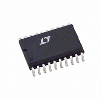
LTC1609CSW#TRPBF Linear Technology, LTC1609CSW#TRPBF Datasheet - Page 16

LTC1609CSW#TRPBF
Manufacturer Part Number
LTC1609CSW#TRPBF
Description
IC ADC SRL 16BIT 200KSPS 20-SOIC
Manufacturer
Linear Technology
Datasheet
1.LTC1609CSW.pdf
(24 pages)
Specifications of LTC1609CSW#TRPBF
Number Of Bits
16
Sampling Rate (per Second)
200k
Data Interface
Serial
Number Of Converters
1
Power Dissipation (max)
100mW
Voltage Supply Source
Analog and Digital
Operating Temperature
0°C ~ 70°C
Mounting Type
Surface Mount
Package / Case
20-SOIC (0.300", 7.50mm Width)
Lead Free Status / RoHS Status
Lead free / RoHS Compliant
Available stocks
Company
Part Number
Manufacturer
Quantity
Price
APPLICATIO S I FOR ATIO
LTC1609
External Data Clock Data Read After the Conversion
Figure 10 shows how the result from the current conver-
sion can be read out after the conversion has been com-
pleted. The externally supplied data clock is running
continuously. CS and R/C are first used together to initiate
a conversion and then CS is used to read the result. The
conversion starts on the falling edge of CS with R/C low.
Both CS and R/C should be returned high within 1.2 s to
prevent the transition from disturbing the conversion.
After the conversion has been completed (BUSY returning
high), a pulse on the SYNC pin will be generated after the
first rising edge of DATACLK #1 that occurs after CS goes
low (R/C high). The SYNC output can be captured on the
falling edge of DATACLK #1 or on the rising edge of
DATACLK #2. After the rising edge of DATACLK #2, the
SYNC output will go low and the MSB will be clocked out
on the DATA pin. This bit can be latched on the falling edge
of DATACLK #2 or on the rising edge of DATACLK #3. The
LSB will be valid on the falling edge of DATACLK #17 or the
rising edge of DATACLK #18. After the rising edge of
DATACLK #18 the DATA pin will take on the value of the
TAG pin that occurred at the rising edge of DATACLK #2.
16
EXTERNAL
DATACLK
BUSY
SYNC
DATA
TAG
R/C
CS
Figure 10. Conversion and Read Timing with External Clock (EXT/INT Tied High). Read After Conversion
t
16
t
t
1
2
U
U
t
t
3
13
W
t
16
t
15
0
t
17
t
12
1
U
t
t
t
TAG0
14
12
23
2
(MSB)
TAG1
B15
t
t
18
24
3
Using the highest frequency permitted for DATACLK
(20MHz), shifting the data out after the conversion will not
degrade the 200kHz throughput.
External Discontinuous Data Clock Data Read
During the Conversion
Figure 11 shows how the result from the previous conver-
sion can be read out during the current conversion. The
externally supplied data clock is running discontinuously.
R/C is used to initiate a conversion with CS tied low. The
conversion starts on the falling edge of R/C. R/C should be
returned high within 1.2 s to prevent the transition from
disturbing the conversion. A pulse on the SYNC pin will be
generated on rising edge of DATACLK #0. The SYNC
output can be captured on the falling edge of DATACLK #0
or on the rising edge of DATACLK #1. After the rising edge
of DATACLK #1, the SYNC output will go low and the MSB
will be clocked out on the DATA pin. This bit can be latched
on the falling edge of DATACLK #1 or on the rising edge of
DATACLK #2. The LSB will be valid on the falling edge of
DATACLK #16. Another clock pulse would be needed if the
LSB is captured on a rising edge. A minimum of 17 clock
pulses are required if the data is captured on falling clock
edges.
TAG2
B14
4
TAG15
B1
17
TAG16
B0
18
TAG17
TAG0
t
19
TAG18
TAG1
TAG19
1606 F10
1609fa


