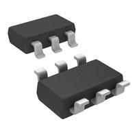
ADC101C021CIMKX/NOPB National Semiconductor, ADC101C021CIMKX/NOPB Datasheet - Page 20

ADC101C021CIMKX/NOPB
Manufacturer Part Number
ADC101C021CIMKX/NOPB
Description
IC ADC 10BIT SAR I2C TSOT-23-6
Manufacturer
National Semiconductor
Datasheet
1.ADC101C021CIMMNOPB.pdf
(30 pages)
Specifications of ADC101C021CIMKX/NOPB
Number Of Bits
10
Sampling Rate (per Second)
188.9k
Data Interface
I²C, Serial
Number Of Converters
1
Power Dissipation (max)
780µW
Voltage Supply Source
Single Supply
Operating Temperature
-40°C ~ 105°C
Mounting Type
Surface Mount
Package / Case
SOT-23-6 Thin, TSOT-23-6
For Use With
ADC101C02XEB - BOARD EVALUATION FOR ADC101C02X
Lead Free Status / RoHS Status
Lead free / RoHS Compliant
Other names
ADC101C021CIMKX
www.national.com
1.6.9 V
This register holds the Highest Conversion result when in the Automatic mode. Each conversion result is compared against the
contents of this register. If the value is higher, it replaces the previous value. If the value is lower, the register contents remain
unchanged. The highest conversion value can be cleared at any time by writing 0000h to this register. The value of this register
will update automatically when the automatic conversion mode is enabled, but is NOT updated in the normal mode.
Pointer Address 07h (Read/Write)
Default Value: 0000h
1.7 SERIAL INTERFACE
The I
modes. Standard mode (100kHz) and Fast mode (400kHz)
are functionally the same and will be referred to as Standard-
Fast mode in this document. High-Speed mode (3.4MHz) is
an extension of Standard-Fast mode and will be referred to
as Hs-mode in this document.
The following diagrams describe the timing relationships of
the clock (SCL) and data (SDA) signals. Pull-up resistors or
current sources are required on the SCL and SDA busses to
pull them high when they are not being driven low. A logic zero
is transmitted by driving the output low. A logic high is trans-
mitted by releasing the output and allowing it to be pulled-up
externally. The appropriate pull-up resistor values will depend
upon the total bus capacitance and operating speed. The AD-
C101C021 offers extended ESD tolerance (8kV HBM) for the
I
across multiple boards without extra ESD protection.
1.7.1 Basic I
The I
to operate on the same bus. The bus consists of master de-
vices and slave devices which can communicate back and
forth over the I
and are typically microcontrollers, FPGAs, DSPs, or other
digital controllers. Slave devices are controlled by a master
and
ADC101C021. To support multiple devices on the same bus,
each slave has a unique hardware address which is referred
to as the "slave address." To communicate with a particular
device on the bus, the controller (master) sends the slave ad-
dress and listens for a response from the slave. This response
Bits
15:12
11:2
1:0
Bits
15:12
11:2
1:0
2
C bus pins (SCL & SDA) allowing extension of the bus
2
D15
2
C interface is bi-directional and allows multiple devices
D7
D7
are
C-compatible interface operates in all three speed
MAX
Name
Reserved
Lowest Conversion
Reserved
Name
Reserved
Highest Conversion
Reserved
-- Highest Conversion Register
typically
2
C Protocol
2
C interface. Master devices control the bus
D14
D6
D6
peripheral
Reserved
Description
Always reads zeros. Zeros must be written to these bits.
Contains the Lowest Conversion result. D11 is MSB.
Always reads zeros. Zeros must be written to these bits.
Description
Always reads zeros. Zeros must be written to these bits.
Highest conversion result. D11 is MSB.
Always reads zeros. Zeros must be written to these bits.
devices
Highest Conversion [5:0]
Lowest Conversion [5:0]
D13
D5
D5
such
as
D12
D4
D4
the
20
is referred to as an acknowledge bit. If a slave on the bus is
addressed correctly, it Acknowledges (ACKs) the master by
driving the SDA bus low. If the address doesn't match a
device's slave address, it Not-acknowledges (NACKs) the
master by letting SDA be pulled high. ACKs also occur on the
bus when data is being transmitted. When the master is writ-
ing data, the slave ACKs after every data byte is successfully
received. When the master is reading data, the master ACKs
after every data byte is received to let the slave know it wants
to receive another data byte. When the master wants to stop
reading, it NACKs after the last data byte and creates a stop
condition on the bus.
All communication on the bus begins with either a Start con-
dition or a Repeated Start condition. The protocol for starting
the bus varies between Standard-Fast mode and Hs-mode.
In
Start condition by driving SDA from high to low while SCL is
high. In Hs-mode, starting the bus is more complicated.
Please refer to Section 1.7.3 High-Speed (Hs) Mode for the
full details of a Hs-mode Start condition.
A Repeated Start is generated to address a different device
or register, or to switch between read and write modes. The
master generates a Repeated Start condition by driving SDA
low while SCL is high. Following the Repeated Start, the mas-
ter sends out the slave address and a read/write bit as shown
in Figure 7. The bus continues to operate in the same speed
mode as before the Repeated Start condition.
All communication on the bus ends with a Stop condition. In
either Standard-Fast mode or Hs-Mode, a Stop condition oc-
curs when SDA is pulled high while SCL is high. After a Stop
condition, the bus remains idle until a master generates an-
other Start condition.
D11
D3
D3
Standard-Fast
Highest Conversion [9:6]
D10
D2
D2
mode,
the
D1
D9
D1
master
Reserved
Reserved
generates
D0
D8
D0
a


