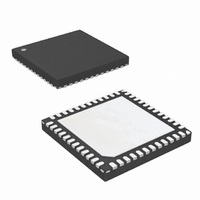
KAD5512P-12Q48 Intersil, KAD5512P-12Q48 Datasheet - Page 6

KAD5512P-12Q48
Manufacturer Part Number
KAD5512P-12Q48
Description
IC ADC 12BIT 125MSPS SGL 48-QFN
Manufacturer
Intersil
Series
FemtoCharge™r
Datasheet
1.KAD5512P-25Q72.pdf
(36 pages)
Specifications of KAD5512P-12Q48
Number Of Bits
12
Sampling Rate (per Second)
125M
Data Interface
Serial, SPI™
Number Of Converters
1
Power Dissipation (max)
235mW
Voltage Supply Source
Single Supply
Operating Temperature
-40°C ~ 85°C
Mounting Type
Surface Mount
Package / Case
48-VQFN
For Use With
KDC5512-Q48EVAL - DAUGHTER CARD FOR KAD5512KDC5512EVAL - DAUGHTER CARD FOR KAD5512
Lead Free Status / RoHS Status
Lead free / RoHS Compliant
Pin Descriptions - 48 Ld QFN
NOTE: LVCMOS Output Mode Functionality is shown in brackets (NC = No Connection).
(Exposed Paddle)
1, 9, 13, 17, 47
2-4, 11, 21, 22
PIN NUMBER
5, 8, 12, 48
19, 29, 42
14, 15
20, 37
PAD
6, 7
10
16
18
23
24
25
26
27
28
30
31
32
33
34
35
36
38
39
40
41
43
44
45
46
LVDS [LVCMOS] NAME
6
CLKP, CLKN
VINN, VINP
[CLKOUT]
CLKOUTN
CLKOUTP
RESETN
NAPSLP
RLVDS
OVDD
AVDD
OVSS
AVSS
SDIO
AVSS
SCLK
[NC]
[NC]
[NC]
[NC]
[NC]
[NC]
[NC]
[OR]
VCM
[D0]
[D1]
[D2]
[D3]
[D4]
[D5]
ORN
[NC]
SDO
DNC
D0N
D1N
D2N
D3N
D4N
D5N
ORP
D0P
D1P
D2P
D3P
D4P
D5P
CSB
KAD5512P
1.8V Analog Supply
Do Not Connect
Analog Ground
Analog Input Negative, Positive
Common Mode Output
Clock Input True, Complement
Tri-Level Power Control (Nap, Sleep modes)
Power On Reset (Active Low, see page 19)
Output Ground
1.8V Output Supply
LVDS DDR Logical Bits 1, 0 Output Complement
[NC in LVCMOS]
LVDS DDR Logical Bits 1, 0 Output True
[CMOS DDR Logical Bits 1, 0 in LVCMOS]
LVDS DDR Logical Bits 3, 2 Output Complement
[NC in LVCMOS]
LVDS DDR Logical Bits 3, 2 Output True
[CMOS DDR Logical Bits 3, 2 in LVCMOS]
LVDS DDR Logical Bits 5, 4 Output Complement
[NC in LVCMOS]
LVDS DDR Logical Bits 5, 4 Output True
[CMOS DDR Logical Bits 5, 4 in LVCMOS]
LVDS Bias Resistor (Connect to OVSS with a 10kΩ, 1% resistor)
LVDS Clock Output Complement
[NC in LVCMOS]
LVDS Clock Output True
[LVCMOS CLKOUT]
LVDS DDR Logical Bits 7, 6 Output Complement
[NC in LVCMOS]
LVDS DDR Logical Bits 7, 6 Output True
[CMOS DDR Logical Bits 7, 6 in LVCMOS]
LVDS DDR Logical Bits 9, 8 Output Complement
[NC in LVCMOS]
LVDS DDR Logical Bits 9, 8 Output True
[CMOS DDR Logical Bits 9, 8 in LVCMOS]
LVDS DDR Logical Bits 11, 10 Output Complement
[NC in LVCMOS]
LVDS DDR Logical Bits 11, 10 Output True
[CMOS DDR Logical Bits 11, 10 in LVCMOS]
LVDS Over Range Complement
[NC in LVCMOS]
LVDS Over Range True
[LVCMOS Over Range]
SPI Serial Data Output (4.7kΩ pull-up to OVDD is required)
SPI Chip Select (active low)
SPI Clock
SPI Serial Data Input/Output
Analog Ground (Connect to a low thermal impedance analog
ground plane with multiple vias)
LVDS [LVCMOS] FUNCTION
October 1, 2010
FN6807.4


