ADC14C105CISQX National Semiconductor, ADC14C105CISQX Datasheet
ADC14C105CISQX
Specifications of ADC14C105CISQX


Related parts for ADC14C105CISQX

ADC14C105CISQX Summary of contents
Page 1
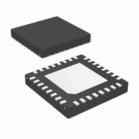
... The ADC14C105 is available in a 32-lead LLP package and operates over the industrial temperature range of −40°C to +85°C. Connection Diagram © 2007 National Semiconductor Corporation Features ■ 1 GHz Full Power Bandwidth ■ Internal reference and sample-and-hold circuit ■ ...
Page 2
Block Diagram Ordering Information Industrial (−40°C www.national.com ≤ ≤ T +85°C) A ADC14C105CISQ ADC14C105CISQE 250-Piece Tape and Reel ADC14C105EB 2 Package 32 Pin LLP 32 Pin LLP, Evaluation Board 30017902 ...
Page 3
Pin Descriptions and Equivalent Circuits Pin No. Symbol ANALOG I CMO REF 12 OF/DCS DIGITAL I/O 11 CLK 30 PD Equivalent Circuit ...
Page 4
Pin No. Symbol 13-19, D0–D13 23-29 21 DRDY ANALOG POWER AGND Exposed Pad DIGITAL POWER DRGND www.national.com Equivalent Circuit Digital data output pins that make up the 14-bit ...
Page 5
... Absolute Maximum Ratings If Military/Aerospace specified devices are required, please contact the National Semiconductor Sales Office/ Distributors for availability and specifications. Supply Voltage ( Voltage on Any Pin (Not to exceed 4.2V) Input Current at Any Pin other than Supply Pins (Note 4) Package Input Current (Note 4) ...
Page 6
Symbol Parameter V Internal Reference bottom RN Ext V External Reference Voltage REF Dynamic Converter Electrical Characteristics Unless otherwise specified, the following specifications apply: AGND = DRGND = 0V, V +1.2V 105 MHz, 50% Duty Cycle, DCS disabled, ...
Page 7
Symbol Parameter C Digital Input Capacitance IN DIGITAL OUTPUT CHARACTERISTICS (D0–D13, DRDY) V Logical “1” Output Voltage OUT(1) V Logical “0” Output Voltage OUT(0) +I Output Short Circuit Source Current SC −I Output Short Circuit Sink Current SC C Digital ...
Page 8
Dynamic Converter Electrical Characteristics at 95MSPS Unless otherwise specified, the following specifications apply: AGND = DRGND = 0V, V +1.2V MHz, 50% Duty Cycle, DCS disabled, V CLK ≤ ≤ . All other limits apply for T ...
Page 9
Note 9: With a full scale differential input of 2V P-P Note 10: Typical figures are 25°C and represent most likely parametric norms at the time of product characterization. The typical specifications are not A guaranteed. Note ...
Page 10
Specification Definitions APERTURE DELAY is the time after the falling edge of the clock to when the input signal is acquired or held for conver- sion. APERTURE JITTER (APERTURE UNCERTAINTY) is the variation in aperture delay from sample to sample. ...
Page 11
Timing Diagram Transfer Characteristic FIGURE 1. Output Timing FIGURE 2. Transfer Characteristic 11 30017909 30017910 www.national.com ...
Page 12
Typical Performance Characteristics DNL, INL specifications apply: AGND = DRGND = 0V, V DCS disabled MHz CMO IN DNL DNL vs. f DNL vs. Temperature www.national.com = +3.3V +2.5V, ...
Page 13
DNL vs 30017949 13 INL vs 30017950 www.national.com ...
Page 14
Typical Performance Characteristics AGND = DRGND = 0V +3.3V MHz pF/pin. Typical values are for T CMO IN L SNR, SINAD, SFDR vs. V SNR, SINAD, SFDR vs. ...
Page 15
SNR, SINAD, SFDR vs. Clock Duty Cycle SNR, SINAD, SFDR vs. Clock Duty Cycle, DCS Enabled SNR, SINAD, SFDR vs. f Distortion vs. Clock Duty Cycle 30017957 Distortion vs. Clock Duty Cycle, DCS Enabled 30017959 IN 30017963 15 30017958 30017960 ...
Page 16
SNR, SINAD, SFDR vs. Temperature Spectral Response @ 10 MHz Input Spectral Response @ 240 MHz Input www.national.com Distortion vs. Temperature 30017965 Spectral Response @ 70 MHz Input 30017968 Intermodulation Distortion, f 30017970 16 30017966 30017969 1= 19.5 MHz, f ...
Page 17
Power vs. f CLK 30017972 17 www.national.com ...
Page 18
Functional Description Operating on a single +3.3V supply, the ADC14C105 uses a pipeline architecture and has error correction circuitry to help ensure maximum performance. The differential analog input signal is digitized to 14 bits. The user has the choice of ...
Page 19
− V − REF CM REF V − REF CM REF − ...
Page 20
It is important that all grounds associated with the reference voltage and the analog input signal make connection to the ground plane at a ...
Page 21
POWER SUPPLY CONSIDERATIONS The power supply pins should be bypassed with a 0.1 µF ca- pacitor and with a 100 pF ceramic chip capacitor close to each power pin. Leadless chip capacitors are preferred because they have low series ...
Page 22
All ground connections should have a low inductance path to ground. 7.0 DYNAMIC PERFORMANCE To achieve the best dynamic performance, the clock source driving the CLK input must have ...
Page 23
Physical Dimensions inches (millimeters) unless otherwise noted 32-Lead LLP Package Ordering Number: ADC14C105CISQ NS Package Number SQA32A 23 www.national.com ...
Page 24
... National Semiconductor and the National Semiconductor logo are registered trademarks of National Semiconductor Corporation. All other brand or product names may be trademarks or registered trademarks of their respective holders. ...