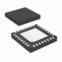
ADC14C105CISQX National Semiconductor, ADC14C105CISQX Datasheet - Page 21

ADC14C105CISQX
Manufacturer Part Number
ADC14C105CISQX
Description
ADC 14BIT 95/105MSPS 32-LLP
Manufacturer
National Semiconductor
Series
PowerWise®r
Datasheet
1.ADC14C105CISQENOPB.pdf
(24 pages)
Specifications of ADC14C105CISQX
Number Of Bits
14
Sampling Rate (per Second)
105M
Data Interface
Serial, Parallel
Number Of Converters
1
Power Dissipation (max)
400mW
Voltage Supply Source
Single Supply
Operating Temperature
-40°C ~ 85°C
Mounting Type
Surface Mount
Package / Case
32-WFQFN Exposed Pad
For Use With
ADC14C105EB - BOARD EVAL 14-BIT ADC14C105
Lead Free Status / RoHS Status
Contains lead / RoHS non-compliant
5.0 POWER SUPPLY CONSIDERATIONS
The power supply pins should be bypassed with a 0.1 µF ca-
pacitor and with a 100 pF ceramic chip capacitor close to each
power pin. Leadless chip capacitors are preferred because
they have low series inductance.
As is the case with all high-speed converters, the AD-
C14C105 is sensitive to power supply noise. Accordingly, the
noise on the analog supply pin should be kept below 100
mV
No pin should ever have a voltage on it that is in excess of the
supply voltages, not even on a transient basis. Be especially
careful of this during power turn on and turn off.
The V
operated from a supply in the range of 2.4V to V
ables lower power operation, reduces the noise coupling
effects from the digital outputs to the analog circuitry and sim-
plifies interfacing to lower voltage devices and systems.
6.0 LAYOUT AND GROUNDING
Proper grounding and proper routing of all signals are essen-
tial to ensure accurate conversion. Maintaining separate ana-
log and digital areas of the board, with the ADC14C105
between these areas, is required to achieve specified perfor-
mance.
The ground return for the data outputs (DRGND) carries the
ground current for the output drivers. The output current can
exhibit high transients that could add noise to the conversion
process. To prevent this from happening, the DRGND pins
should NOT be connected to system ground in close proximity
to any of the ADC14C105's other ground pins.
Capacitive coupling between the typically noisy digital circuit-
ry and the sensitive analog circuitry can lead to poor perfor-
mance. The solution is to keep the analog circuitry separated
from the digital circuitry, and to keep the clock line as short as
possible.
The effects of the noise generated from the ADC output
switching can be minimized through the use of 22Ω resistors
in series with each data output line. Locate these resistors as
close to the ADC output pins as possible.
P-P
DR
.
pin provides power for the output drivers and may be
FIGURE 7. Application Circuit
A
. This en-
21
Since digital switching transients are composed largely of
high frequency components, total ground plane copper
weight will have little effect upon the logic-generated noise.
This is because of the skin effect. Total surface area is more
important than is total ground plane area.
Generally, analog and digital lines should cross each other at
90° to avoid crosstalk. To maximize accuracy in high speed,
high resolution systems, however, avoid crossing analog and
digital lines altogether. It is important to keep clock lines as
short as possible and isolated from ALL other lines, including
other digital lines. Even the generally accepted 90° crossing
should be avoided with the clock line as even a little coupling
can cause problems at high frequencies. This is because oth-
er lines can introduce jitter into the clock line, which can lead
to degradation of SNR. Also, the high speed clock can intro-
duce noise into the analog chain.
Best performance at high frequencies and at high resolution
is obtained with a straight signal path. That is, the signal path
through all components should form a straight line wherever
possible.
Be especially careful with the layout of inductors and trans-
formers. Mutual inductance can change the characteristics of
the circuit in which they are used. Inductors and transformers
should not be placed side by side, even with just a small part
of their bodies beside each other. For instance, place trans-
formers for the analog input and the clock input at 90° to one
another to avoid magnetic coupling.
The analog input should be isolated from noisy signal traces
to avoid coupling of spurious signals into the input. Any ex-
ternal component (e.g., a filter capacitor) connected between
the converter's input pins and ground or to the reference input
pin and ground should be connected to a very clean point in
the ground plane.
All analog circuitry (input amplifiers, filters, reference compo-
nents, etc.) should be placed in the analog area of the board.
All digital circuitry and dynamic I/O lines should be placed in
the digital area of the board. The ADC14C105 should be be-
tween these two areas. Furthermore, all components in the
reference circuitry and the input signal chain that are con-
nected to ground should be connected together with short
www.national.com
30017919


