ADC14C105CISQX National Semiconductor, ADC14C105CISQX Datasheet - Page 5
ADC14C105CISQX
Manufacturer Part Number
ADC14C105CISQX
Description
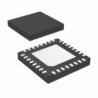
ADC 14BIT 95/105MSPS 32-LLP
Manufacturer
National Semiconductor
Series
PowerWise®r
Datasheet
1.ADC14C105CISQENOPB.pdf
(24 pages)
Specifications of ADC14C105CISQX
Number Of Bits
14
Sampling Rate (per Second)
105M
Data Interface
Serial, Parallel
Number Of Converters
1
Power Dissipation (max)
400mW
Voltage Supply Source
Single Supply
Operating Temperature
-40°C ~ 85°C
Mounting Type
Surface Mount
Package / Case
32-WFQFN Exposed Pad
For Use With
ADC14C105EB - BOARD EVAL 14-BIT ADC14C105
Lead Free Status / RoHS Status
Contains lead / RoHS non-compliant


STATIC CONVERTER CHARACTERISTICS
INL
DNL
PGE
NGE
TC PGE Positive Gain Error Tempco
TC NGE Negative Gain Error Tempco
V
TC V
REFERENCE AND ANALOG INPUT CHARACTERISTICS
V
V
C
V
TC V
V
Symbol
OFF
CMO
CM
REF
RP
IN
Absolute Maximum Ratings
If Military/Aerospace specified devices are required,
please contact the National Semiconductor Sales Office/
Distributors for availability and specifications.
Converter Electrical Characteristics
Unless otherwise specified, the following specifications apply: AGND = DRGND = 0V, V
+1.2V, f
limits apply for T
Supply Voltage (V
Voltage on Any Pin
Input Current at Any Pin other
than Supply Pins (Note 4)
Package Input Current (Note 4)
Max Junction Temp (T
Thermal Resistance (θ
ESD Rating
Storage Temperature
Soldering process must comply with National
Semiconductor's Reflow Temperature Profile
specifications. Refer to www.national.com/packaging.
(Note 7)
OFF
REF
(Not to exceed 4.2V)
Human Body Model (Note 6)
Machine Model (Note 6)
CLK
Resolution with No Missing Codes
Integral Non Linearity
Differential Non Linearity
Positive Gain Error
Negative Gain Error
Offset Error (V
Offset Error Tempco
Under Range Output Code
Over Range Output Code
Common Mode Output Voltage
Analog Input Common Mode Voltage
V
(Note 11)
Internal Reference Voltage
Internal Reference Voltage Tempco
Internal Reference top
IN
= 105 MHz, 50% Duty Cycle, DCS disabled, V
Input Capacitance (each pin to GND)
MIN
A
, V
≤
IN
DR
Parameter
J
JA
T
)
+ = V
)
A
)
≤
T
IN
MAX
-)
. All other limits apply for T
−0.3V to (V
−65°C to +150°C
−0.3V to 4.2V
(Notes 1, 3)
−40°C
−40°C
−40°C
V
± 0.5 V
−40°C
(Note 13)
A
±50 mA
30°C/W
IN
+150°C
+0.3V)
±5 mA
2500V
= 1.5 Vdc
250V
≤
≤
≤
≤
CM
T
T
T
T
A
A
A
A
A
= V
≤
≤
≤
≤
= 25°C (Notes 8, 9)
5
CMO
+85°C
+85°C
+85°C
+85°C
Conditions
Operating Ratings
, C
Operating Temperature
Supply Voltage (V
Output Driver Supply (V
Clock Duty Cycle
V
|AGND-DRGND|
CM
L
(CLK LOW)
(CLK HIGH)
= 5 pF/pin. Typical values are for T
(DCS Enabled)
(DCS disabled)
A
A
)
= +3.3V, V
(Note 10)
DR
Typical
16383
0.065
-0.05
-0.54
±1.8
±0.5
1.18
1.98
)
7.5
1.5
1.5
8.5
3.5
18
-8
-7
0
DR
(Notes 1, 3)
= +2.5V, Internal V
Limits
16383
±1.25
±1.25
±0.55
1.56
1.89
2.06
-0.9
1.3
1.4
1.4
1.6
14
-4
−40°C
4
0
A
= 25°C. Boldface
+2.7V to +3.6V
≤
1.4V to 1.6V
+2.4V to V
T
%FS (max)
%FS (max)
%FS (max)
LSB (max)
LSB (max)
www.national.com
LSB (min)
LSB (min)
Bits (min)
A
(Limits)
V (max)
V (max)
V (max)
ppm/°C
ppm/°C
ppm/°C
ppm/°C
V (min)
V (min)
V (min)
≤
≤
Units
30/70 %
45/55 %
100mV
pF
pF
+85°C
V
REF
=
A
Related parts for ADC14C105CISQX
Image
Part Number
Description
Manufacturer
Datasheet
Request
R

Part Number:
Description:
National Semiconductor [8-Bit D/A Converter]
Manufacturer:
National Semiconductor
Datasheet:
Part Number:
Description:
National Semiconductor [Media Coprocessor]
Manufacturer:
National Semiconductor
Datasheet:
Part Number:
Description:
Digitally Controlled Tone and Volume Circuit with Stereo Audio Power Amplifier, Microphone Preamp Stage and National 3D Sound
Manufacturer:
National Semiconductor
Datasheet:
Part Number:
Description:
Digitally Controlled Tone and Volume Circuit with Stereo Audio Power Amplifier, Microphone Preamp Stage and National 3D Sound
Manufacturer:
National Semiconductor
Datasheet:
Part Number:
Description:
AC97 Rev 2 Codec with Sample Rate Conversion and National 3D Sound
Manufacturer:
National Semiconductor
Part Number:
Description:
Manufacturer:
National Semiconductor
Datasheet:
Part Number:
Description:
Manufacturer:
National Semiconductor
Datasheet:
Part Number:
Description:
General Purpose, Low Voltage, Low Power, Rail-to-Rail Output Operational Amplifiers
Manufacturer:
National Semiconductor
Datasheet:
Part Number:
Description:
8-bit 20 MSPS flash A/D converter.
Manufacturer:
National Semiconductor
Datasheet:
Part Number:
Description:
Low Noise Quad Operational Amplifier
Manufacturer:
National Semiconductor
Datasheet:
Part Number:
Description:
Quad Differential Line Receivers
Manufacturer:
National Semiconductor
Datasheet:
Part Number:
Description:
Quad High Speed Trapezoidal? Bus Transceiver
Manufacturer:
National Semiconductor
Datasheet:
Part Number:
Description:
Dual Line Receiver
Manufacturer:
National Semiconductor
Datasheet:
Part Number:
Description:
TTL to 10k ECL Level Translator with Latch
Manufacturer:
National Semiconductor
Datasheet: