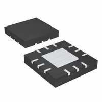
MAX1274BETC+ Maxim Integrated Products, MAX1274BETC+ Datasheet - Page 15

MAX1274BETC+
Manufacturer Part Number
MAX1274BETC+
Description
IC ADC 12BIT 1.8MSPS 12-TQFN
Manufacturer
Maxim Integrated Products
Datasheet
1.MAX1274BETCT.pdf
(18 pages)
Specifications of MAX1274BETC+
Number Of Bits
12
Sampling Rate (per Second)
1.8M
Data Interface
MICROWIRE™, QSPI™, Serial, SPI™
Number Of Converters
1
Power Dissipation (max)
45mW
Voltage Supply Source
Analog and Digital
Operating Temperature
-40°C ~ 85°C
Mounting Type
Surface Mount
Package / Case
12-WQFN Exposed Pad
Lead Free Status / RoHS Status
Lead free / RoHS Compliant
The SPC register should be written as follows:
This setup allows continuous conversion, provided that
the DRR is serviced before the next conversion.
Alternatively, autobuffering can be enabled when using
the buffered serial port to read the data without CPU
TXM = 0, external frame sync
MCM = 0, CLKX is taken from the CLKX pin
FSM = 1, burst mode
FO = 0, data transmitted/received as 16-bit words
Figure 15. Interfacing to the TMS320C54_ Internal Clocks
Figure 16. Interfacing to the TMS320C54_ External Clocks
Figure 17. DSP Interface—Continuous Conversion
CNVST
DOUT
SCLK
MAX1274
MAX1275
MAX1274
MAX1275
D0
CONVERT
CLOCK
CNVST
0
CNVST
DOUT
SCLK
DOUT
SCLK
______________________________________________________________________________________
V
V
L
L
1
0
0
1.8Msps, Single-Supply, Low-Power,
0
DV
CLKR
FSR
DR
DV
CLKX
CLKR
FSX
FSR
DR
DD
DD
TMS320C54_
D11
TMS320C54_
D10
True-Differential, 12-Bit ADCs
D9
D8
D7
intervention. Connect the V
supply
MAX1275 are operating with an analog supply voltage
higher than the DSP supply voltage.
The MAX1274/MAX1275 can also be connected to the
TMS320C54_ by using the data transmit (DX) pin to
drive CNVST and the CLKX generated internally to
drive SCLK. A pullup resistor is required on the CNVST
signal to keep it high when DX goes high impedance
and 0001hex should be written to the DXR continuously
for continuous conversions. The power-down modes
may be entered by writing 00FFhex to the DXR (see
Figures 17 and 18).
The MAX1274/MAX1275 can be directly connected to
the ADSP21_ _ _ family of DSPs from Analog Devices,
Inc. Figure 19 shows the direct connection of the
MAX1274/MAX1275 to the ADSP21_ _ _. There are two
modes of operation that can be programmed to interface
with the MAX1274/MAX1275. For continuous conver-
sions, idle CNVST low and pulse it high for one clock
cycle during the LSB of the previous transmitted word.
The ADSP21_ _ _ STCTL and SRCTL registers should be
configured for early framing (LAFR = 0) and for an
active-high frame (LTFS = 0, LRFS = 0) signal. In this
mode, the data-independent frame-sync bit (DITFS = 1)
can be selected to eliminate the need for writing to the
transmit-data register more than once. For single conver-
sions, idle CNVST high and pulse it low for the entire
conversion. The ADSP21_ _ _ STCTL and SRCTL regis-
ters should be configured for late framing (LAFR = 1)
and for an active-low frame (LTFS = 1, LRFS = 1) signal.
This is also the best way to enter the power-down modes
by setting the word length to 8 bits (SLEN = 1001).
Connect the V
when the MAX1274/MAX1275 are operating with a sup-
ply voltage higher than the DSP supply voltage (see
Figures 17 and 18).
D6
D5
voltage
DSP Interface to the ADSP21_ _ _
L
pin to the ADSP21_ _ _ supply voltage
D4
D3
when
D2
L
pin to the TMS320C54_
D1
the
D0
MAX1274/
0
1
0
15


