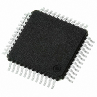
TSA1401IF STMicroelectronics, TSA1401IF Datasheet - Page 14

TSA1401IF
Manufacturer Part Number
TSA1401IF
Description
IC ADC 14BIT 20MSPS 85MW 48TQFP
Manufacturer
STMicroelectronics
Datasheet
1.TSA1401IF.pdf
(19 pages)
Specifications of TSA1401IF
Number Of Bits
14
Sampling Rate (per Second)
20M
Data Interface
Parallel
Power Dissipation (max)
85mW
Voltage Supply Source
Analog and Digital
Operating Temperature
-40°C ~ 85°C
Mounting Type
Surface Mount
Package / Case
48-TQFP, 48-VQFP
Lead Free Status / RoHS Status
Lead free / RoHS Compliant
Other names
497-4458
Available stocks
Company
Part Number
Manufacturer
Quantity
Price
Company:
Part Number:
TSA1401IF
Manufacturer:
STMicroelectronics
Quantity:
10 000
TSA1401
sampling capacitor will draw/inject a small current
transient on the input signal.
One method to mask this transient current is a
low-pass RC filter as shown on
Figure 17
the
mounted in parallel of the two analog inputs
signals will absorb the transient glitches.
Fig. 15: ADC input equivalent circuit
Single-ended signal with transformer:
Using an RF transformer is a good means to
achieve high performance.
Figures 16
signal is fed to the primary of the transformer,
while the secondary drives both ADC inputs.
Fig. 16: Differential input configuration with
The internal common mode voltage of the ADC
(INCM) is connected to the center-tap of the
secondary of the transformer in order to bias the
input
internally set to 0.46V. The INCM is decoupled to
maintain a low noise level on this node.
AC coupled differential input:
Figure 17
input signal in AC-coupled differential input
14/19
Analog source
sampling
VIN
signal around
transformer
50
. A larger capacitor value compared to
represents the biasing of a differential
describes the schematics. The input
AGND
AVcc
ADT1-1
capacitor
1:1
Z
Cin=4pF
in
=1/(2 Cs.Fs)=3.3k (Fs=20MHz)
this
330pF
100pF
(appoximately
common
10nF
VINB
Figures 16
INCM
VIN
TSA1401
4.7µF
INCM
voltage,
2pF)
and
configuration. Both inputs VIN and VINB are
centered around the common mode voltage CM,
that can be forced through INCM or supplied
externally (in this case the internal common mode
of the TSA1401 may be left internal at 0.45V,
different from the input common mode value).
Fig. 17: AC-coupled differential input
5.2 - Clock management
The converter performances are very dependant
on clock input accuracy, in terms of aperture delay
and jitter. The voltage error induced by the jitter of
the clock is:
V
where T
ADC) and,
SR is the slew rate of the input signal:
SR max=2 .F
frequency)
V
missing codes. At the end we have:
V
T
For TSA1401 at 10MHz input frequency, we have
T
performances of the TSA1401, the clock applied
should have a jitter below 1ps.
The clock power supplies must be separated from
the ADC output ones to avoid digital noise
modulation at the output.
It is strongly advised not to switch off the clock
when the circuit is active (power supply on).
mode
common
j
j
error
error
error
<FS/(2 .Fs.F
<1ps. Consequently to target the maximum
50
50
=SR.T
=2 .F
should be less than an LSB to guarantee no
j
is the jitter of the clock (system clock and
10nF
10nF
33pF
in
j
,
.FS.T
APPLICATION INFORMATION
in
.FS (FS full scale, F
in
.2
100k
100k
j
n
and Verror< FS/2
).
INCM
VIN
VINB
TSA1401
in
n
input signal


