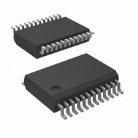
ADC12H034CIMSA/NOPB National Semiconductor, ADC12H034CIMSA/NOPB Datasheet - Page 37

ADC12H034CIMSA/NOPB
Manufacturer Part Number
ADC12H034CIMSA/NOPB
Description
ADC 12BIT W/S&H +SIGN 24-SSOP
Manufacturer
National Semiconductor
Datasheet
1.ADC12030CIWMNOPB.pdf
(42 pages)
Specifications of ADC12H034CIMSA/NOPB
Number Of Bits
12
Data Interface
NSC MICROWIRE™, Serial
Number Of Converters
4
Power Dissipation (max)
33mW
Voltage Supply Source
Analog and Digital
Operating Temperature
-40°C ~ 85°C
Mounting Type
Surface Mount
Package / Case
24-SSOP (0.200", 5.30mm Width)
Number Of Elements
1
Architecture
SAR
Input Polarity
Unipolar
Input Type
Voltage
Rated Input Volt
5V
Differential Input
Yes
Power Supply Requirement
Analog and Digital
Single Supply Voltage (typ)
5V
Single Supply Voltage (min)
4.5V
Single Supply Voltage (max)
5.5V
Dual Supply Voltage (typ)
Not RequiredV
Dual Supply Voltage (min)
Not RequiredV
Dual Supply Voltage (max)
Not RequiredV
Power Dissipation
500mW
Differential Linearity Error
±1LSB
Integral Nonlinearity Error
±1LSB
Operating Temp Range
-40C to 85C
Operating Temperature Classification
Industrial
Mounting
Surface Mount
Pin Count
24
Package Type
SSOP
Lead Free Status / RoHS Status
Lead free / RoHS Compliant
Other names
ADC12H034CIMSA
The assignment of the RS-232 port is shown below
A sample program, written in Microsoft QuickBasic, is shown
on the next page. The program prompts for data mode select
instruction to be sent to the ADC. This can be found from the
Mode Programming table shown earlier. The data should be
entered in “1”s and “0”s as shown in the table with DI0 first.
Next, the program prompts for the number of SCLK cycles
required for the programmed mode select instruction. For in-
stance, to send all “0”s to the ADC, selects CH0 as the +input,
CH1 as the −input, 12-bit conversion, and 13-bit MSB first
data output format (if the sign bit was not turned off by a pre-
vious instruction). This would require 13 SCLK periods since
the output data format is 13 bits.
The ADC powers up with No Auto Cal, No Auto Zero, 10
CCLK Acquisition Time, 12-bit conversion, data out with sign,
COM1
Input Address
Output Address
3FC
3FE
B7
X
X
37
B6
X
X
power up, 12- or 13-bit MSB first, and user mode. Auto Cal,
Auto Zero, Power Up and Power Down instructions do not
change these default settings. The following power up se-
quence should be followed:
1.
2.
3.
It is recommended that the first instruction issued to the
ADC12038 be Auto Cal (see Section 1.1 Interface Con-
cepts).
B5
X
X
Run the program
Prior to responding to the prompt apply the power to the
ADC12038
Respond to the program prompts
CTS
B4
0
B3
X
X
B2
X
X
RTS
B1
X
DTR
B0
X
www.national.com


