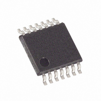
MAX5478EUD+ Maxim Integrated Products, MAX5478EUD+ Datasheet - Page 13

MAX5478EUD+
Manufacturer Part Number
MAX5478EUD+
Description
IC POT DGTL DUAL 256-TAP 14TSSOP
Manufacturer
Maxim Integrated Products
Datasheet
1.MAX5477ETE.pdf
(17 pages)
Specifications of MAX5478EUD+
Taps
256
Resistance (ohms)
50K
Number Of Circuits
2
Temperature Coefficient
35 ppm/°C Typical
Memory Type
Non-Volatile
Interface
I²C, 2-Wire Serial
Voltage - Supply
2.7 V ~ 5.25 V
Operating Temperature
-40°C ~ 85°C
Mounting Type
Surface Mount
Package / Case
14-TSSOP
Resistance In Ohms
50K
Number Of Pots
Dual
Taps Per Pot
256
Resistance
325 Ohms
Wiper Memory
Non Volatile
Digital Interface
Serial (2-Wire)
Operating Supply Voltage
2.7 V to 5.25 V
Supply Current
1 uA
Maximum Operating Temperature
+ 85 C
Minimum Operating Temperature
- 40 C
Description/function
Dual, 256 Tap, Nonvolatile, I2C, 50k Digital Potentiometer
Mounting Style
SMD/SMT
Supply Voltage (max)
5.25 V
Supply Voltage (min)
2.7 V
Tolerance
25 %
Lead Free Status / RoHS Status
Lead free / RoHS Compliant
3 bits in the slave address. Connect each address input
to V
have a unique address to share a common bus.
Write to the MAX5477/MAX5478/MAX5479 by transmit-
ting the device’s slave address with NOP/W (8th bit) set
to zero, followed by at least 1 byte of information
(Figure
byte. The bytes received after the command byte are
the data bytes. The 1st data byte goes into the internal
register of the MAX5477/MAX5478/MAX5479 as select-
ed by the command byte
Figure 5. Bit Transfer
Figure 7. Command Byte Received
Figure 8. Command and Single Data Byte Received
SDA
SCL
S
DD
HOW CONTROL BYTE AND DATA BYTE MAP INTO
or GND to set these 3 bits. Each device must
7). The 1st byte of information is the command
S
MAX5477/MAX5478/MAX5479 REGISTERS
DATA STABLE,
DATA VALID
SLAVE ADDRESS
COMMAND BYTE IS STORED ON RECEIPT OF STOP CONDITION
Dual, 256-Tap, Nonvolatile, I
MAX5477/MAX5478/MAX5479
______________________________________________________________________________________
Message Format for Writing
CHANGE OF
DATA ALLOWED
ACKNOWLEDGE FROM
SLAVE ADDRESS
(Figure
NOP/W
MAX5477/MAX5478/MAX5479
8).
0
ACKNOWLEDGE FROM
A
D15 D14 D13 D12 D11 D10
NOP/W
0
MAX5477/MAX5478/MAX5479
COMMAND BYTE
ACKNOWLEDGE FROM
A
D15
Use the command byte to select the source and desti-
nation of the wiper data (nonvolatile or volatile memory
registers) and swap data between nonvolatile and
volatile memory registers (see
VREG: The data byte writes to the volatile memory reg-
ister and the wiper position updates with the data in the
volatile memory register.
NVREG: The data byte writes to the nonvolatile memory
register. The wiper position is unchanged.
NVREGxVREG: Data transfers from the nonvolatile
memory register to the volatile memory register (wiper
position updates).
Figure 6. Acknowledge
Digital Potentiometers
SDA
SCL
CONDITION
D14
D9
START
D13
D8
COMMAND BYTE
A
D12
1
D7
MAX5477/MAX5478/MAX5479
D11
D6
2
ACKNOWLEDGE FROM
D10
D5
MAX5477/MAX5478/MAX5479
2
C-Interface,
DATA BYTE
D4
1 BYTE
ACKNOWLEDGE FROM
D9
NOT ACKNOWLEDGE
Table
Command Descriptions
D3
ACKNOWLEDGE
D8
D2
8
ACKNOWLEDGMENT
3).
CLOCK PULSE FOR
Command Byte
A
D1
D0
9
P
A
P
13


