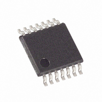
MAX5478EUD+ Maxim Integrated Products, MAX5478EUD+ Datasheet - Page 4

MAX5478EUD+
Manufacturer Part Number
MAX5478EUD+
Description
IC POT DGTL DUAL 256-TAP 14TSSOP
Manufacturer
Maxim Integrated Products
Datasheet
1.MAX5477ETE.pdf
(17 pages)
Specifications of MAX5478EUD+
Taps
256
Resistance (ohms)
50K
Number Of Circuits
2
Temperature Coefficient
35 ppm/°C Typical
Memory Type
Non-Volatile
Interface
I²C, 2-Wire Serial
Voltage - Supply
2.7 V ~ 5.25 V
Operating Temperature
-40°C ~ 85°C
Mounting Type
Surface Mount
Package / Case
14-TSSOP
Resistance In Ohms
50K
Number Of Pots
Dual
Taps Per Pot
256
Resistance
325 Ohms
Wiper Memory
Non Volatile
Digital Interface
Serial (2-Wire)
Operating Supply Voltage
2.7 V to 5.25 V
Supply Current
1 uA
Maximum Operating Temperature
+ 85 C
Minimum Operating Temperature
- 40 C
Description/function
Dual, 256 Tap, Nonvolatile, I2C, 50k Digital Potentiometer
Mounting Style
SMD/SMT
Supply Voltage (max)
5.25 V
Supply Voltage (min)
2.7 V
Tolerance
25 %
Lead Free Status / RoHS Status
Lead free / RoHS Compliant
TIMING CHARACTERISTICS (continued)
(V
T
Dual, 256-Tap, Nonvolatile, I
Digital Potentiometers
4
Note 1: All devices are production tested at T
Note 2: The DNL and INL are measured with the potentiometer configured as a voltage-divider with H_ = V
Note 3: The DNL and INL are measured with the potentiometer configured as a variable resistor. H_ is unconnected and L_ =
Note 4: The wiper resistance is measured using the source currents given in Note 3.
Note 5: The devices draw current in excess of the specified supply current when the digital inputs are driven with voltages between
Note 6: Wiper at midscale with a 10pF load (DC measurement). L_ = GND, an AC source is applied to H_, and the W_ output is
Note 7: The programming current exists only during power-up and EEPROM writes.
Note 8: The SCL clock period includes rise and fall times (t
Note 9: Digital timing is guaranteed by design and characterization, and is not production tested.
Note 10: This is measured from the STOP pulse to the time it takes the output to reach 50% of the output step size (divider mode). It
Note 11: An appropriate bus pullup resistance must be selected depending on board capacitance. Refer to the I
Note 12: The idle time begins from the initiation of the STOP pulse.
A
SCL High Time
SCL Low Time
Data Setup Time
Data Hold Time
SDA, SCL Rise Time
SDA, SCL Fall Time
Setup Time for STOP Condition
Bus Free Time Between STOP
and START Condition
Pulse Width of Spike Suppressed
Capacitive Load for Each Bus
Line
Write NV Register Busy Time
DD
= +25°C. See Figure 1.) (Notes 8 and 9)
_______________________________________________________________________________________
= +2.7V to +5.25V, H_ = V
wiper terminal is unloaded and measured with a high-input-impedance voltmeter.
GND. For V
the wiper is driven with 200µA (MAX5477), 40µA (MAX5478), or 20µA (MAX5479).
(V
measured. A 3dB bandwidth occurs when the AC W_/H_ value is 3dB lower than the DC W_/H_ value.
timed from a voltage level of (V
is measured with a maximum external capacitive load of 10pF.
tion document linked to this web address: www.semiconductors.philips.com/acrobat/literature/9398/39340011.pdf
PARAMETER
DD
- 0.5V) and (GND + 0.5V). See Supply Current vs. Digital Input Voltage in the Typical Operating Characteristics.
DD
= +5V, the wiper is driven with 400µA (MAX5477), 80µA (MAX5478), or 40µA (MAX5479). For V
DD
, L_ = GND, T
SYMBOL
t
t
t
HD:DAT
SU:DAT
SU:STO
t
t
HIGH
t
LOW
BUF
t
C
IL
t
t
SP
R
F
B
+ V
A
IH
= +25°C and are guaranteed by design and characterization for -40°C < T
) / 2.
Minimum power-up rate = 0.2V/µs
(Note 11)
(Note 12)
A
= -40°C to +85°C, unless otherwise noted. Typical values are at V
R
CONDITIONS
= t
F
). All digital input signals are specified with t
2
C-Interface,
MIN
100
0.6
1.3
0.6
1.3
0
TYP
DD
and L_ = GND. The
R
2
MAX
C-bus specifica-
300
300
400
0.9
50
12
= t
F
A
= 2ns and
DD
DD
< +85°C.
UNITS
= +5V,
= +3V,
ms
pF
µs
µs
ns
µs
ns
ns
µs
µs
ns


