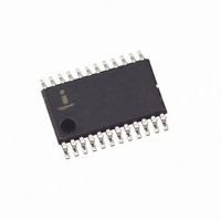
X9408WV24IZ-2.7T1 Intersil, X9408WV24IZ-2.7T1 Datasheet

X9408WV24IZ-2.7T1
Specifications of X9408WV24IZ-2.7T1
Related parts for X9408WV24IZ-2.7T1
X9408WV24IZ-2.7T1 Summary of contents
Page 1
... L1 CAUTION: These devices are sensitive to electrostatic discharge; follow proper IC Handling Procedures. 1-888-INTERSIL or 1-888-468-3774 XDCP is a trademark of Intersil Americas Inc. Copyright Intersil Americas Inc. 2005, 2009. All Rights Reserved All other trademarks mentioned are the property of their respective owners. X9408 Low Noise/Low Power/2-Wire Bus FN8191 ...
Page 2
... X9408WV24I-2.7* X9408WV G X9408WV24IZ-2.7* (Note) X9408WV Z G *Add "T1" suffix for tape and reel. **Add "T1" suffix for tape and reel.Please refer to TB347 for details on reel specifications. NOTE: These Intersil Pb-free plastic packaged products employ special Pb-free material sets, molding compounds/die attach materials, and 100% matte tin plate plus anneal (e3 termination finish, which is RoHS compliant and compatible with both SnPb and Pb-free soldering operations) ...
Page 3
Pin Descriptions Host Interface Pins SERIAL CLOCK (SCL) The SCL input is used to clock data into and out of the X9408. SERIAL DATA (SDA) SDA is a bidirectional pin used to transfer data into and out of the device. ...
Page 4
Principals of Operation The X9408 is a highly integrated microcircuit incorporating four resistor arrays and their associated registers and counters and the serial interface logic providing direct communication between the host and the XDCP potentiometers. Serial Interface The X9408 supports ...
Page 5
Flow 1. ACK Polling Sequence NON-VOLATILE WRITE COMMAND COMPLETED ENTER ACK POLLING ISSUE START ISSUE SLAVE ADDRESS ACK NO RETURNED? YES NO FURTHER OPERATION? YES ISSUE INSTRUCTION PROCEED Instruction Structure The next byte sent to the X9408 contains the instruction ...
Page 6
The Increment/Decrement command is different from the other commands. Once the command is issued and the X9408 has responded with an acknowledge, the master can clock the selected wiper up and/or down in one segment steps; thereby, providing a fine ...
Page 7
INC/DEC CMD ISSUED SCL SDA FIGURE 6. INCREMENT/DECREMENT TIMING LIMITS SCL FROM MASTER DATA OUTPUT FROM TRANSMITTER DATA OUTPUT FROM RECEIVER START FIGURE 7. ACKNOWLEDGE RESPNSE FROM RECEIVER 7 X9408 VOLTAGE OUT 1 t WRID 8 ...
Page 8
SERIAL DATA PATH FROM INTERFACE CIRCUITRY REGISTER 0 REGISTER 2 IF WCR = 00[H] THEN WCR = 3F[H] THEN FIGURE 8. ...
Page 9
TABLE 3. WIPER COUNTER REGISTER, (6-BIT), VOLATILE WP5 WP4 WP3 WP2 (MSB) Instruction Format NOTES: 1. “MACK”/”SACK”: stands for the acknowledge sent by the master/slave. 2. “A3 ~ A0”: stands for the device addresses sent by ...
Page 10
Write Wiper Counter Register (WCR) to Data Register (DR) S DEVICE TYPE DEVICE T IDENTIFIER ADDRESSES Increment/Decrement Wiper Counter Register (WCR) S DEVICE TYPE DEVICE T IDENTIFIER ADDRESSES A 0 ...
Page 11
... W W Current 11 X9408 Thermal Information Temperature Under Bias . . . . . . . . . . . . . . . . . . . . .-65°C to +135°C Storage Temperature . . . . . . . . . . . . . . . . . . . . . . . .-65°C to +150°C Pb-Free Reflow Profile .see link below http://www.intersil.com/pbfree/Pb-FreeReflow.asp Operating Conditions Temperature Range Commercial . . . . . . . . . . . . . . . . . . . . . . . . . . . . . . . 0°C to +70°C Industrial .-40°C to +85°C TEST CONDITION +25°C, each pot ...
Page 12
DC Electrical Specifications SYMBOL PARAMETER I V supply current (nonvolatile write) CC1 supply current (move wiper, write, CC2 CC read current (standby Input leakage current ...
Page 13
Power-up Requirements (Power-up sequencing can affect correct recall of the wiper registers). The preferred power-on sequence is as follows: First V-, then V and V+, and then the potentiometer pins and Voltage ...
Page 14
AC Timing SYMBOL f Clock frequency SCL t Clock cycle time CYC t Clock high time HIGH t Clock low time LOW t Start setup time SU:STA t Start hold time HD:STA t Stop setup time ...
Page 15
Timing Diagrams Start and Stop Timing g (START) SCL t SU:STA SDA Input Timing t CYC SCL SDA t SU:DAT Output Timing SCL SDA XDCP Timing (for All Load Instructions) SCL SDA VWx 15 X9408 ...
Page 16
XDCP Timing (for Increment/Decrement Instruction) SCL SDA WIPER REGISTER ADDRESS VWx Write Protect and Device Address Pins Timing SCL SDA WP A0, A1 A2, A3 Applications information Basic Configurations of Electronic Potentiometers V R THREE TERMINAL POTENTIOMETER; VARIABLE VOLTAGE DIVIDER ...
Page 17
Application Circuits NONINVERTING AMPLIFIER – (1 OFFSET VOLTAGE ADJUSTMENT 100kΩ – + TL072 10kΩ 10kΩ 10kΩ +12V -12V 17 ...
Page 18
Application Circuits (continued) ATTENUATOR – All -1/2 ≤ G ≤ +1/2 INVERTING AMPLIFIER – ...
Page 19
Plastic Packages for Intergrated Circuits Thin Shrink Small Outline Package Family (TSSOP (N/2)+ (N/2) B TOP VIEW e C SEATING PLANE b 0.10 0. LEADS SIDE VIEW SEE ...
Page 20
... Accordingly, the reader is cautioned to verify that data sheets are current before placing orders. Information furnished by Intersil is believed to be accurate and reliable. However, no responsibility is assumed by Intersil or its subsidiaries for its use; nor for any infringements of patents or other rights of third parties which may result from its use ...


