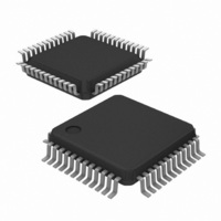
LTC2757BILX#PBF Linear Technology, LTC2757BILX#PBF Datasheet - Page 11

LTC2757BILX#PBF
Manufacturer Part Number
LTC2757BILX#PBF
Description
IC DAC 18BIT PAR 48LQFP
Manufacturer
Linear Technology
Series
SoftSpan™r
Datasheet
1.LTC2757BILXPBF.pdf
(20 pages)
Specifications of LTC2757BILX#PBF
Settling Time
2.1µs
Number Of Bits
18
Data Interface
Parallel
Number Of Converters
1
Voltage Supply Source
Single Supply
Operating Temperature
-40°C ~ 85°C
Mounting Type
Surface Mount
Package / Case
48-LQFP
Lead Free Status / RoHS Status
Lead free / RoHS Compliant
Power Dissipation (max)
-
Available stocks
Company
Part Number
Manufacturer
Quantity
Price
OPERATION
Output Ranges
The LTC2757 is a current-output, parallel-input precision
multiplying DAC offering ±1LSB INL and DNL over six
software-selectable output ranges. Ranges can either
be programmed in software for maximum fl exibility or
hardwired through pin-strapping. Two unipolar ranges
are available (0V to 5V and 0V to 10V), and four bipolar
ranges (±2.5V, ±5V, ±10V and –2.5V to 7.5V). These ranges
are obtained when an external precision 5V reference is
used. The output ranges for other reference voltages
are easy to calculate by observing that each range is a
multiple of the external reference voltage. The ranges can
then be expressed: 0 to 1×, 0 to 2×, ±0.5×, ±1×, ±2×, and
–0.5× to 1.5×.
Digital Section
The LTC2757 has four internal interface registers (see
Block Diagram). Two of these—one Input and one DAC
register—are dedicated to the Data I/O port, and two
to the Span I/O port. Each port is thus double buffered.
Double buffering provides the capability to simultaneously
update the Span and Code registers, which allows smooth
voltage transitions when changing output ranges. It also
permits the simultaneous updating of multiple DACs or
other parts on the data bus.
Write and Update Operations
Load the data input register directly from an 18-bit bus
by holding the D/S pin low and then pulsing the WR pin
low (Write operation).
Load the Span Input register by holding the D/S pin high
and then pulsing the WR pin low (Write operation). The
Span and Data register structures are the same except for
the number of parallel bits—the Span registers have three
bits, while the Data registers have 18 bits.
The DAC registers are loaded by pulsing the UPD pin
high (Update operation), which copies the data held in
the Input registers of both ports into the DAC registers.
Note that Update operations always include both Data
and Span registers; but the DAC register values will not
change unless the Input register values have previously
been changed by a Write operation.
To make both registers transparent for fl owthrough
mode, tie WR low and UPD high. However, this defeats
the deglitcher operation and output glitch impulse may
increase. The deglitcher is activated on the rising edge
of the UPD pin.
The interface also allows the use of the Input and DAC
registers in a master-slave, or edge-triggered, confi gura-
tion. This mode of operation occurs when WR and UPD
are tied together and driven by a single clock signal. The
data bits are loaded into the Input register on the falling
edge of the clock and then loaded into the DAC register
on the rising edge.
It is possible to control both ports on one 18-bit wide
data bus by allowing Span pins S2 to S0 to share bus
lines with the Data LSBs (D2 to D0). No Write or Read
operation acts on both span and data, so there cannot be
a signal confl ict.
The asynchronous clear pin (CLR) resets the LTC2757
to 0V (zero-, half- or quarter-scale code) in any output
range. CLR resets both the Input and DAC data registers,
but leaves the Span registers unchanged.
The device also has a power-on reset that initializes the DAC
to V
the 0V to 5V range at zero-scale if the part is in SoftSpan
confi guration. For manual span (M-SPAN tied to V
Manual Span Confi guration ), the DACs power-up in the
manually-chosen range at the appropriate code.
Manual Span Confi guration
Multiple output ranges are not needed in some applica-
tions. To confi gure the LTC2757 for single-span opera-
tion, tie the M-SPAN pin to V
The desired output range is programmed by tying S0,
S1 and S2 to GND or V
this confi guration, no range-setting software routine is
needed; the part will initialize to the chosen output range
at power-up, with V
When confi gured for manual span operation, Span port
readback is disabled.
OUT
= 0V in any output range. The DAC powers up in
OUT
DD
= 0V.
(see Figure 1 and Table 2). In
DD
and the D/S pin to GND.
LTC2757
11
DD
; see
2757f


