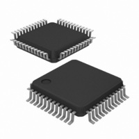
LTC2757BILX#PBF Linear Technology, LTC2757BILX#PBF Datasheet - Page 12

LTC2757BILX#PBF
Manufacturer Part Number
LTC2757BILX#PBF
Description
IC DAC 18BIT PAR 48LQFP
Manufacturer
Linear Technology
Series
SoftSpan™r
Datasheet
1.LTC2757BILXPBF.pdf
(20 pages)
Specifications of LTC2757BILX#PBF
Settling Time
2.1µs
Number Of Bits
18
Data Interface
Parallel
Number Of Converters
1
Voltage Supply Source
Single Supply
Operating Temperature
-40°C ~ 85°C
Mounting Type
Surface Mount
Package / Case
48-LQFP
Lead Free Status / RoHS Status
Lead free / RoHS Compliant
Power Dissipation (max)
-
Available stocks
Company
Part Number
Manufacturer
Quantity
Price
LTC2757
OPERATION
Readback
The contents of any one of the four interface registers can
be read back from the I/O ports by using the READ pin in
conjunction with the D/S and UPD pins.
The I/O pins and registers are grouped into two ports—Data
and Span. The Data I/O port consists of pins D0-D17, and
the Span I/O port consists of pins S0, S1 and S2.
Each I/O port has one dedicated Input register and one
dedicated DAC register. The register structure is shown
in the Block Diagram.
A Readback operation is initiated by asserting READ to
logic high after selecting the desired I/O port.
Select the I/O port (Data or Span) to be read back with
the D/S pin. The selected I/O port’s pins become logic
outputs during readback, while the unselected I/O port’s
pins remain high-impedance digital inputs.
With the I/O port selected, assert READ high and select
the desired Input or DAC register using the UPD pin. Note
that UPD is a two function pin—the Update function is only
available when READ is low. If READ is high, the Update
function is disabled and the UPD pin instead functions
as a register selector, selecting an Input or DAC register
for readback. Table 1 shows the readback functions for
the LTC2757.
Table 1. Write, Update and Read Functions
READ D/S
X = Don’t Care
12
0
0
0
0
0
0
0
0
1
1
1
1
0
0
0
0
1
1
1
1
0
0
1
1
WR UPD
0
0
1
1
0
0
1
1
X
X
X
X
0
1
0
1
0
1
0
1
0
1
0
1
Write to Input Register
Update DAC Register
Update DAC register
Read Input Register
Read DAC Register
Write/Update
(Transparent)
SPAN I/O
-
-
-
-
-
-
Write to Input Register
Update DAC Register
Update DAC Register
Read Input Register
Read DAC Register
(Transparent)
Write/Update
DATA I/O
-
-
-
-
-
-
The most common readback task is to check the contents
of an Input register after writing to it, and before updating
the new data to the DAC register. To do this, hold UPD low
and assert READ high. The contents of the selected port’s
Input register are output to its I/O pins.
To read back the contents of a DAC register, hold UPD low
and assert READ high, then bring UPD high to select the
DAC register. The contents of the selected DAC register are
output by the selected port’s I/O pins. Note: if no update is
desired after the readback operation, UPD must be returned
low before bringing READ low, otherwise the UPD pin will
revert to its primary function and update the DAC.
Table 2. Span Codes
Codes not shown are reserved and should not be used.
System Offset and Gain Adjustments
Many systems require compensation for overall system
offset. This may be an order of magnitude or more greater
than the offset of the LTC2757, which is so low as to be
dominated by external output amplifi er errors even when
using the most precise op amps.
S2
0
0
0
0
1
1
S1
0
0
1
1
0
0
2757 F01
Figure 1. Confi guring the LTC2757 for
Single-Span Operation (±10V Range)
S0
0
1
0
1
0
1
M-SPAN
S2
S1
S0
D/S
SPAN
Unipolar 0V to 5V
Unipolar 0V to 10V
Bipolar –5V to 5V
Bipolar –10V to 10V
Bipolar –2.5V to 2.5V
Bipolar –2.5V to 7.5V
WR
UPD
LTC2757
V
V
DD
DD
READ
DATA I/O
18
2757f


