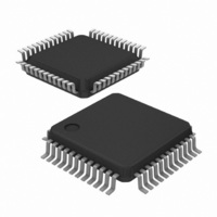
LTC2757BILX#PBF Linear Technology, LTC2757BILX#PBF Datasheet - Page 17

LTC2757BILX#PBF
Manufacturer Part Number
LTC2757BILX#PBF
Description
IC DAC 18BIT PAR 48LQFP
Manufacturer
Linear Technology
Series
SoftSpan™r
Datasheet
1.LTC2757BILXPBF.pdf
(20 pages)
Specifications of LTC2757BILX#PBF
Settling Time
2.1µs
Number Of Bits
18
Data Interface
Parallel
Number Of Converters
1
Voltage Supply Source
Single Supply
Operating Temperature
-40°C ~ 85°C
Mounting Type
Surface Mount
Package / Case
48-LQFP
Lead Free Status / RoHS Status
Lead free / RoHS Compliant
Power Dissipation (max)
-
Available stocks
Company
Part Number
Manufacturer
Quantity
Price
APPLICATIONS INFORMATION
swing to ±10V at the output. Compensation is taken from
the output of the LTC6240, allowing the use of a much larger
compensation capacitor than if taken after the gain-of-fi ve
stage. An LTC2054 auto-zero amplifi er senses the voltage
at I
to eliminate the offset of the high speed path. The 100:1
attenuator and input fi lter reduce the low frequency noise
in this stage while maintaining low DC offset.
Precision Voltage Reference Considerations
Much in the same way selecting an operational amplifi er
for use with the LTC2757 is critical to the performance of
the system, selecting a precision voltage reference also
requires due diligence. The output voltage of the LTC2757
is directly affected by the voltage reference; thus, any
voltage reference error will appear as a DAC output volt-
age error.
There are three primary error sources to consider when
selecting a precision voltage reference for 18-bit appli-
cations: output voltage initial tolerance, output voltage
temperature coeffi cient and output voltage noise.
Initial reference output voltage tolerance, if uncorrected,
generates a full-scale error term. Choosing a reference
with low output voltage initial tolerance, like the LT1236
(±0.05%), minimizes the gain error caused by the reference;
however, a calibration sequence that corrects for system
zero- and full-scale error is always recommended.
A reference’s output voltage temperature coeffi cient affects
not only the full-scale error, but can also affect the circuit’s
INL and DNL performance. If a reference is chosen with
a loose output voltage temperature coeffi cient, then the
DAC output voltage along its transfer characteristic will
be very dependent on ambient conditions. Minimizing
the error due to reference temperature coeffi cient can be
achieved by choosing a precision reference with a low
output voltage temperature coeffi cient and/or tightly con-
trolling the ambient temperature of the circuit to minimize
temperature gradients.
As precision DAC applications move to 18-bit performance,
reference output voltage noise may contribute a dominant
share of the system’s noise fl oor. This in turn can degrade
system dynamic range and signal-to-noise ratio. Care
OUT1
and drives the non-inverting input of the LTC6240
should be exercised in selecting a voltage reference with
as low an output noise voltage as practical for the system
resolution desired. Precision voltage references like the
LT1236 produce low output noise in the 0.1Hz to 10Hz
region, well below the 18-bit LSB level in 5V or 10V full-
scale systems. However, as the circuit bandwidths increase,
fi ltering the output of the reference may be required to
minimize output noise.
Table 6. Partial List of LTC Precision References Recommended
for Use with the LTC2757 with Relevant Specifi cations
REFERENCE
LT1019A-5,
LT1019A-10
LT1236A-5,
LT1236A-10
LT1460A-5,
LT1460A-10
LT1790A-2.5
LTC6655-2.5
LTC6655-5
Grounding
As with any high-resolution converter, clean grounding is
important. A low-impedance analog ground plane is nec-
essary, as are star grounding techniques. Keep the board
layer used for star ground continuous to minimize ground
resistances; that is, use the star-ground concept without
using separate star traces. The I
concern; INL will be degraded by the code-dependent
currents carried by the I
drops to ground are allowed to develop. The best strategy
here is to tie the pins to the star ground plane by multiple
vias located directly underneath the part. Alternatively, the
pins may be routed to the star ground point if necessary;
join them together at the part and route a single trace of
no more than 30 squares of 1oz copper.
In the rare case in which neither of these alternatives is
practicable, a force/sense amplifi er should be used as a
ground buffer (see the Typical Applications section). Note,
however, that the voltage offset of the ground buffer amp
directly contributes to the effects on accuracy specifi ed in
Table 4 under ‘V
can be calculated by substituting the total offset from I
to I
OUT2S
for V
OS1
TOLERANCE
OS1
±0.075%
±0.025%
±0.05%
±0.05%
±0.05%
INITIAL
in the equations.
Max
Max
Max
Max
Max
’. The combined effects of the offsets
OUT2F
TEMPERATURE
and I
OUT2
10ppm/°C
10ppm/°C
5ppm/°C
5ppm/°C
2ppm/°C
DRIFT
Max
Max
Max
Max
Max
OUT2S
pins are of particular
LTC2757
pins if voltage
0.1Hz to 10Hz
0.62μV
12μV
20μV
12μV
3μV
NOISE
17
P-P
P-P
P-P
P-P
P-P
OUT1
2757f


