LTC2757BILX#PBF Linear Technology, LTC2757BILX#PBF Datasheet - Page 5
LTC2757BILX#PBF
Manufacturer Part Number
LTC2757BILX#PBF
Description
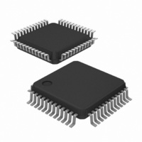
IC DAC 18BIT PAR 48LQFP
Manufacturer
Linear Technology
Series
SoftSpan™r
Datasheet
1.LTC2757BILXPBF.pdf
(20 pages)
Specifications of LTC2757BILX#PBF
Settling Time
2.1µs
Number Of Bits
18
Data Interface
Parallel
Number Of Converters
1
Voltage Supply Source
Single Supply
Operating Temperature
-40°C ~ 85°C
Mounting Type
Surface Mount
Package / Case
48-LQFP
Lead Free Status / RoHS Status
Lead free / RoHS Compliant
Power Dissipation (max)
-
Available stocks
Company
Part Number
Manufacturer
Quantity
Price


TIMING CHARACTERISTICS
Note 1: Stresses beyond those listed under Absolute Maximum Ratings
may cause permanent damage to the device. Exposure to any Absolute
Maximum Rating condition for extended periods may affect device
reliability and lifetime.
Note 2: Continuous operation above the specifi ed maximum operating
junction temperature may impair device reliability.
Note 3: Temperature Coeffi cient is calculated by dividing the maximum
change in the parameter by the specifi ed temperature range.
Note 4: R1 is measured from R
R
Note 5: Parallel combination of the resistances from REF to I
REF to I
Note 6: Because of the proprietary SoftSpan switching architecture, the
measured resistance looking into each of the specifi ed pins is constant for
all output ranges if the I
SYMBOL
CLR Timing
t
V
Write and Update Timing
t
t
t
t
t
t
t
t
Readback Timing
t
t
t
t
t
t
t
t
t
t
CLR Timing
t
apply over the full operating temperature range, otherwise specifi cations are at T
25
1
2
3
4
5
6
7
8
13
14
15
17
18
19
20
22
23
24
25
DD
COM
= 2.7V to 3.3V
.
OUT2
. DAC input resistance is independent of code.
PARAMETER
CLR Pulse Width Low
I/O Valid to WR Rising Edge Set-Up
I/O Valid to WR Rising Edge Hold
WR Pulse Width
UPD Pulse Width
UPD Falling Edge to WR Falling Edge
WR Rising Edge to UPD Rising Edge
D/S Valid to WR Falling Edge Set-Up Time
WR Rising Edge to D/S Valid Hold Time
WR Rising Edge to Read Rising Edge
Read Falling Edge to WR Falling Edge
Read Rising Edge to I/O Propagation Delay
UPD Valid to I/O Propagation Delay
D/S Valid to Read Rising Edge
Read Rising Edge to UPD Rising Edge
UPD Falling Edge to Read Falling Edge
READ Falling Edge to UPD Rising Edge
I/O Bus Hi-Z to Read Rising Edge
Read Falling Edge to I/O Bus Active
CLR Pulse Width Low
OUT1
and I
IN
to R
OUT2
COM
pins are held at ground.
; R2 is measured from REF to
V
OUT1
DD
CONDITIONS
No Data Shoot-Through
(Note 12)
(Note 12)
C
C
(Note 12)
No Update
No Update
(Note 12)
(Note 12)
(Note 12)
= 5V, V(R
L
L
and from
= 10pF
= 10pF
IN
) = 5V unless otherwise specifi ed. The
Note 7: Using LT1468 with C
of 1.8μs can be achieved by optimizing the time constant on an individual
basis. See Application Note 120, 1ppm Settling Time Measurement for a
Monolithic 18-Bit DAC .
Note 8: Measured at the major carry transition, 0V to 5V range. Output
amplifi er: LT1468; C
Note 9: Zero-code to full-code transition; REF = 0V. Falling transition is
similar or better.
Note 10: REF = 6V
amplifi er = LT1468.
Note 11: Calculation from V
(Boltzmann constant), R = resistance (Ω), T = temperature (°K), and B =
bandwidth (Hz).
Note 12: Guaranteed by design. Not production tested.
A
= 25°C.
RMS
FB
= 50pF .
at 1kHz. 0V to 5V range. DAC code = FS. Output
n
FEEDBACK
= √4kTRB, where k = 1.38E-23 J/°K
l
l
l
l
l
l
l
l
l
l
l
l
l
l
l
l
l
l
l
l
MIN
20
18
18
30
30
18
18
18
40
18
18
40
30
= 27pF . A ±0.0004% settling time
0
0
9
9
0
l
denotes specifi cations that
TYP
LTC2757
MAX
48
48
UNITS
5
2757f
ns
ns
ns
ns
ns
ns
ns
ns
ns
ns
ns
ns
ns
ns
ns
ns
ns
ns
ns
ns
Related parts for LTC2757BILX#PBF
Image
Part Number
Description
Manufacturer
Datasheet
Request
R

Part Number:
Description:
CD ROM LINEARVIEW DATASHEETS
Manufacturer:
Linear Technology

Part Number:
Description:
Standalone Linear Li-Ion Battery Charger with Thermal Regulation in ThinSOT
Manufacturer:
Linear Technology Corporation
Datasheet:
Part Number:
Description:
Low noise, high frequency, 8th order linear phase lowpass filter
Manufacturer:
Linear Technology Corporation
Datasheet:
Part Number:
Description:
Manufacturer:
Linear Technology Corporation
Datasheet:
Part Number:
Description:
Manufacturer:
Linear Technology Corporation
Datasheet:
Part Number:
Description:
Manufacturer:
Linear Technology Corporation
Datasheet:
Part Number:
Description:
Manufacturer:
Linear Technology Corporation
Datasheet:
Part Number:
Description:
Manufacturer:
Linear Technology Corporation
Datasheet:
Part Number:
Description:
Manufacturer:
Linear Technology Corporation
Datasheet:
Part Number:
Description:
Manufacturer:
Linear Technology Corporation
Datasheet:
Part Number:
Description:
Dual and Quad, JFET Input Precision High Speed Op Amps
Manufacturer:
Linear Technology Corporation
Datasheet:
Part Number:
Description:
Manufacturer:
Linear Technology Corporation
Datasheet:
Part Number:
Description:
1, 2, 6 and 8 Channel, 10-Bit Serial I/O Data Acquisition Systems
Manufacturer:
Linear Technology Corporation
Datasheet:
Part Number:
Description:
Manufacturer:
Linear Technology Corporation
Datasheet:
Part Number:
Description:
Universal dual filter building block
Manufacturer:
Linear Technology Corporation
Datasheet: