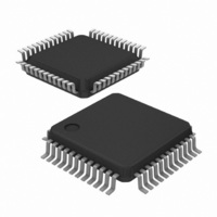
LTC2757BILX#PBF Linear Technology, LTC2757BILX#PBF Datasheet - Page 8

LTC2757BILX#PBF
Manufacturer Part Number
LTC2757BILX#PBF
Description
IC DAC 18BIT PAR 48LQFP
Manufacturer
Linear Technology
Series
SoftSpan™r
Datasheet
1.LTC2757BILXPBF.pdf
(20 pages)
Specifications of LTC2757BILX#PBF
Settling Time
2.1µs
Number Of Bits
18
Data Interface
Parallel
Number Of Converters
1
Voltage Supply Source
Single Supply
Operating Temperature
-40°C ~ 85°C
Mounting Type
Surface Mount
Package / Case
48-LQFP
Lead Free Status / RoHS Status
Lead free / RoHS Compliant
Power Dissipation (max)
-
Available stocks
Company
Part Number
Manufacturer
Quantity
Price
PIN FUNCTIONS
LTC2757
R
Inverting Amplifi er. Normally tied to the external reference
voltage. Typically 5V; accepts up to ±15V. These pins are
internally shorted together.
S2 (Pin 3): Span I/O Bit 2. Pins S0, S1 and S2 are used
to program and to read back the output range of the DAC.
See Table 2.
GND (Pins 4, 7, 18, 19): Ground. Tie to ground.
I
ment Sense and Force Pins. Tie to ground via a clean,
low-impedance path. These pins may also be used with
a precision ground buffer amp as a Kelvin sensing pair
(see the Typical Applications section).
D17-D9 (Pins 8-16): DAC Input/Output Data Bits. These
I/O pins set and read back the DAC code. D17 (Pin 8) is
the MSB.
V
Requires a 0.1μF bypass capacitor to GND.
CLR (Pin 20): Asynchronous Clear Input. When CLR is
asserted low, the DAC output resets to V
LTC2757 selects the appropriate reset code according to
the active output range—zero-scale for 0V to 5V and 0V
to 10V spans, half scale for ±2.5V, ±5V and ±10V spans,
or quarter scale for –2.5V to 7.5V span.
M-SPAN (Pin 21): Manual Span Control Input. M-SPAN
can be pin-strapped to confi gure the LTC2757 for opera-
tion in a single, fi xed output range.
To confi gure the part for single-span use, tie M-SPAN
directly to V
pin strapping; and the Span I/O port ignores Write, Update
and Read commands.
If M-SPAN is instead connected to ground (SoftSpan
confi guration), the output ranges are set and verifi ed by
using Write, Update and Read operations. See Manual
Span Confi guration in the Operation section. M-SPAN
must be connected either directly to GND (for SoftSpan
operation) or V
8
OUT2S
DD
IN
(Pins 1, 2): Input Resistor for External Reference
(Pin 17): Positive Supply Input. 2.7V ≤ V
, I
OUT2F
DD
. The output range is then set via hardware
(Pins 5, 6): DAC Output Current Comple-
DD
(for single-span operation).
OUT
= 0V. The
DD
≤ 5.5V.
DNC (Pins 22, 32): Do Not Connect.
D8-D0 (Pins 23-31): DAC Input/Output Data Bits. These
I/O pins set and read back the DAC code. D0 is the LSB.
D/S (Pin 33): Data/Span Select Input. This pin is used to
select activation of the Data (D/S = 0) or Span (D/S = 1)
Input I/O pins (D0 to D17 or S0 to S2, respectively),
along with their respective dedicated registers, for Write
or Read operations. Update operations are unaffected by
D/S, since all updates affect both Data and Span registers.
For single-span operation, tie D/S to GND.
READ (Pin 34): Read Input. When READ is asserted high,
the Data I/O pins (D0-D17) or Span I/O pins (S0-S2) out-
put the contents of a selected Input or DAC register (see
Table 1). Data/Span ports are selected for readback with
the D/S pin; the Input/DAC registers within those ports
are selected for readback with the UPD pin. The readback
function of the Span I/O pins is disabled when M-SPAN
is tied to V
UPD (Pin 35): Update/Register Select Input.
READ = low: Update function. When UPD is asserted
high, the contents of the Input registers are copied into
their respective DAC registers. The output of the DAC is
updated, refl ecting the new DAC register values.
READ = high: Register selector function. The Update func-
tion is disabled and the UPD pin functions as a register
selector. UPD = low selects Input registers for readback,
high selects DAC registers. See Readback in the Opera-
tion section.
WR (Pin 36): Active-Low Write Input. A Write operation
copies the data present on the Data or Span I/O pins (D0-
D17 or S0-S2, respectively) into the Input register. The
Write function is disabled when READ is high.
S0 (Pin 37): Span I/O Bit 0. Pins S0, S1 and S2 are used
to program and to read back the output range of the DAC.
See Table 2.
S1 (Pin 38): Span I/O Bit 1. Pins S0, S1 and S2 are used
to program and to read back the output range of the DAC.
See Table 2.
DD
.
2757f


