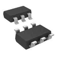
DAC101S101QCMKX/NOPB National Semiconductor, DAC101S101QCMKX/NOPB Datasheet - Page 14

DAC101S101QCMKX/NOPB
Manufacturer Part Number
DAC101S101QCMKX/NOPB
Description
DAC RRO 10BIT MICROPWR TSOT23-6
Manufacturer
National Semiconductor
Series
PowerWise®r
Datasheet
1.DAC101S101CIMKNOPB.pdf
(20 pages)
Specifications of DAC101S101QCMKX/NOPB
Settling Time
8µs
Number Of Bits
10
Data Interface
Serial
Number Of Converters
1
Voltage Supply Source
Single Supply
Power Dissipation (max)
1.41mW
Operating Temperature
-40°C ~ 125°C
Mounting Type
Surface Mount
Package / Case
TSOT-23-6, TSOT-6
Lead Free Status / RoHS Status
Lead free / RoHS Compliant
Other names
DAC101S101QCMKX
Available stocks
Company
Part Number
Manufacturer
Quantity
Price
www.national.com
1.0 Functional Description
1.1 DAC SECTION
The DAC101S101 is fabricated on a CMOS process with an
architecture that consists of a resistor string and switches that
are followed by an output buffer. The power supply serves as
the reference voltage. The input coding is straight binary with
an ideal output voltage of:
where D is the decimal equivalent of the binary code that is
loaded into the DAC register and can take on any value be-
tween 0 and 1023.
1.2 RESISTOR STRING
The resistor string is shown in
of 1024 equal valued resistors in series with a switch at each
junction of two resistors, plus a switch to ground. The code
loaded into the DAC register determines which switch is
closed, connecting the proper node to the amplifier. This con-
figuration guarantees that the DAC is monotonic.
1.3 OUTPUT AMPLIFIER
The output buffer amplifier is a rail-to-rail type, providing an
output voltage range of 0V to V
rail types, exhibit a loss of linearity as the output approaches
the supply rails (0V and V
linearity is specified over less than the full output range of the
DAC. The output capabilities of the amplifier are described in
the Electrical Tables.
1.4 SERIAL INTERFACE
The three-wire interface is compatible with SPI, QSPI and
MICROWIRE as well as most DSPs. See the Timing Diagram
for information on a write sequence.
A write sequence begins by bringing the SYNC line low. Once
SYNC is low, the data on the D
bit serial input register on the falling edges of SCLK. On the
16th falling clock edge, the last data bit is clocked in and the
programmed function (a change in the mode of operation and/
or a change in the DAC register contents) is executed. At this
point the SYNC line may be kept low or brought high. In either
FIGURE 3. DAC Resistor String
V
OUT
= V
A
A
, in this case). For this reason,
x (D / 1024)
Figure
A
IN
. All amplifiers, even rail-to-
line is clocked into the 16-
3. This string consists
20154107
14
case, it must be brought high for the minimum specified time
before the next write sequence so that a falling edge of
SYNC can initiate the next write cycle.
Since the SYNC and D
are high, they should be idled low between write sequences
to minimize power consumption.
1.5 INPUT SHIFT REGISTER
The input shift register,
two bits are "don't cares" and are followed by two bits that
determine the mode of operation (normal mode or one of
three power-down modes). The contents of the serial input
register are transferred to the DAC register on the sixteenth
falling edge of SCLK. See Timing Diagram,
Normally, the SYNC line is kept low for at least 16 falling
edges of SCLK and the DAC is updated on the 16th SCLK
falling edge. However, if SYNC is brought high before the 16th
falling edge, the shift register is reset and the write sequence
is invalid. The DAC register is not updated and there is no
change in the mode of operation.
1.6 POWER-ON RESET
The power-on reset circuit controls the output voltage during
power-up. The DAC register is filled with zeros and the output
voltage is 0 Volts and remains there until a valid write se-
quence is made to the DAC.
1.7 POWER-DOWN MODES
The DAC101S101 has four modes of operation. These
modes are set with two bits (DB13 and DB12) in the control
register.
When both DB13 and DB12 are 0, the device operates nor-
mally. For the other three possible combinations of these bits
the supply current drops to its power-down level and the out-
put is pulled down with either a 1kΩ or a 100KΩ resistor, or
is in a high impedance state, as described in
The bias generator, output amplifier, the resistor string and
other linear circuitry are all shut down in any of the power-
down modes. However, the contents of the DAC register are
unaffected when in power-down. Minimum power consump-
tion is achieved in the power-down mode with SCLK disabled
and SYNC and D
(Wake-Up Time) is typically t
Timing Characteristics Table.
DB13
0
0
1
1
FIGURE 4. Input Register Contents
DB12
TABLE 1. Modes of Operation
0
1
0
1
IN
idled low. The time to exit power-down
Operating Mode
Normal Operation
Power-Down with 1kΩ to GND
Power-Down with 100kΩ to GND
Power-Down with Hi-Z
IN
buffers draw more current when they
Figure
WU
µsec as stated in the A.C. and
4, has sixteen bits. The first
Figure
Table
2.
1.
20154108


