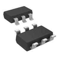
DAC101S101QCMKX/NOPB National Semiconductor, DAC101S101QCMKX/NOPB Datasheet - Page 15

DAC101S101QCMKX/NOPB
Manufacturer Part Number
DAC101S101QCMKX/NOPB
Description
DAC RRO 10BIT MICROPWR TSOT23-6
Manufacturer
National Semiconductor
Series
PowerWise®r
Datasheet
1.DAC101S101CIMKNOPB.pdf
(20 pages)
Specifications of DAC101S101QCMKX/NOPB
Settling Time
8µs
Number Of Bits
10
Data Interface
Serial
Number Of Converters
1
Voltage Supply Source
Single Supply
Power Dissipation (max)
1.41mW
Operating Temperature
-40°C ~ 125°C
Mounting Type
Surface Mount
Package / Case
TSOT-23-6, TSOT-6
Lead Free Status / RoHS Status
Lead free / RoHS Compliant
Other names
DAC101S101QCMKX
Available stocks
Company
Part Number
Manufacturer
Quantity
Price
2.0 Applications Information
The simplicity of the DAC101S101 implies ease of use. How-
ever, it is important to recognize that any data converter that
utilizes its supply voltage as its reference voltage will have
essentially zero PSRR (Power Supply Rejection Ratio).
Therefore, it is necessary to provide a noise-free supply volt-
age to the device.
2.1 DSP/MICROPROCESSOR INTERFACING
Interfacing the DAC101S101 to microprocessors and DSPs
is quite simple. The following guidelines are offered to hasten
the design process.
2.1.1 ADSP-2101/ADSP2103 Interfacing
Figure 5
and the ADSP-2101/ADSP2103. The DSP should be set to
operate in the SPORT Transmit Alternate Framing Mode. It is
programmed through the SPORT control register and should
be configured for Internal Clock Operation, Active Low Fram-
ing and 16-bit Word Length. Transmission is started by writing
a word to the Tx register after the SPORT mode has been
enabled.
2.1.2 80C51/80L51 Interface
A serial interface between the DAC101S101 and the
80C51/80L51 microcontroller is shown in
SYNC signal comes from a bit-programmable pin on the mi-
crocontroller. The example shown here uses port line P3.3.
This line is taken low when data is to transmitted to the
DAC101S101. Since the 80C51/80L51 transmits 8-bit bytes,
only eight falling clock edges occur in the transmit cycle. To
load data into the DAC, the P3.3 line must be left low after the
first eight bits are transmitted. A second write cycle is initiated
to transmit the second byte of data, after which port line P3.3
is brought high. The 80C51/80L51 transmit routine must rec-
ognize that the 80C51/80L51 transmits data with the LSB first
while the DAC101S101 requires data with the MSB first.
2.1.3 68HC11 Interface
A serial interface between the DAC101S101 and the 68HC11
microcontroller is shown in
DAC101S101 is driven from a port line (PC7 in the figure),
similar to the 80C51/80L51.
The 68HC11 should be configured with its CPOL bit as a zero
and its CPHA bit as a one. This configuration causes data on
shows a serial interface between the DAC101S101
FIGURE 5. ADSP-2101/2103 Interface
FIGURE 6. 80C51/80L51 Interface
Figure
7. The SYNC line of the
Figure
20154109
6. The
20154110
15
the MOSI output to be valid on the falling edge of SCLK. PC7
is taken low to transmit data to the DAC. The 68HC11 trans-
mits data in 8-bit bytes with eight falling clock edges. Data is
transmitted with the MSB first. PC7 must remain low after the
first eight bits are transferred. A second write cycle is initiated
to transmit the second byte of data to the DAC, after which
PC7 should be raised to end the write sequence.
2.1.4 Microwire Interface
Figure 8
device and the DAC101S101. Data is clocked out on the rising
edges of the SCLK signal.
2.2 USING REFERENCES AS POWER SUPPLIES
Recall the need for a quiet supply source for devices that use
their power supply voltage as a reference voltage.
Since the DAC101S101 consumes very little power, a refer-
ence source may be used as the supply voltage. The advan-
tages of using a reference source over a voltage regulator are
accuracy and stability. Some low noise regulators can also be
used for the power supply of the DAC101S101. Listed below
are a few power supply options for the DAC101S101.
2.2.1 LM4130
The LM4130 reference, with its 0.05% accuracy over tem-
perature, is a good choice as a power source for the
DAC101S101. Its primary disadvantage is the lack of a 3V
and 5V versions. However, the 4.096V version is useful if a 0
to 4.095V output range is desirable or acceptable. Bypassing
the VIN pin with a 0.1µF capacitor and the VOUT pin with a
2.2µF capacitor will improve stability and reduce output noise.
The LM4130 comes in a space-saving 5-pin SOT23.
FIGURE 9. The LM4130 as a power supply
shows an interface between a Microwire compatible
FIGURE 8. Microwire Interface
FIGURE 7. 68HC11 Interface
www.national.com
20154113
20154111
20154112


