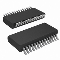
ISL5961IAZ Intersil, ISL5961IAZ Datasheet - Page 4

ISL5961IAZ
Manufacturer Part Number
ISL5961IAZ
Description
CONV D/A 14-BIT 3.3V 28-TSSOP
Manufacturer
Intersil
Datasheet
1.ISL5961IAZ.pdf
(13 pages)
Specifications of ISL5961IAZ
Number Of Bits
14
Data Interface
Parallel
Number Of Converters
1
Voltage Supply Source
Analog and Digital
Power Dissipation (max)
120mW
Operating Temperature
-40°C ~ 85°C
Mounting Type
Surface Mount
Package / Case
28-TSSOP
Lead Free Status / RoHS Status
Lead free / RoHS Compliant
Settling Time
-
Absolute Maximum Ratings
Digital Supply Voltage DV
Analog Supply Voltage AV
Grounds, ACOM TO DCOM. . . . . . . . . . . . . . . . . . . . -0.3V to +0.3V
Digital Input Voltages (D9-D0, CLK, SLEEP). . . . . . . . DV
Reference Input Voltage Range . . . . . . . . . . . . . . . . . . AV
Analog Output Current (I
Operating Conditions
Temperature Range . . . . . . . . . . . . . . . . . . . . . . . . . . -40
CAUTION: Stresses above those listed in “Absolute Maximum Ratings” may cause permanent damage to the device. This is a stress only rating and operation of the
device at these or any other conditions above those indicated in the operational sections of this specification is not implied.
NOTE:
Electrical Specifications
SYSTEM PERFORMANCE
Resolution
Integral Linearity Error, INL
Differential Linearity Error, DNL
Offset Error, I
Offset Drift Coefficient
Full Scale Gain Error, FSE
Full Scale Gain Drift
Full Scale Output Current, I
Output Voltage Compliance Range
DYNAMIC CHARACTERISTICS
Maximum Clock Rate, f
Maximum Clock Rate, f
Output Rise Time
Output Fall Time
Output Capacitance
Output Noise
AC CHARACTERISTICS (Using Figure 13 with R
Spurious Free Dynamic Range,
SFDR Within a Window
1. θ
JA
is measured with the component mounted on an evaluation PC board in free air.
PARAMETER
OS
CLK
CLK
OUT
DD
DD
FS
) . . . . . . . . . . . . . . . . . . . . . . . . . 24mA
to DCOM . . . . . . . . . . . . . . . . . . +3.6V
to ACOM . . . . . . . . . . . . . . . . . . +3.6V
4
AV
DD
“Best Fit” Straight Line (Note 7)
(Note 7)
IOUTA (Note 7)
(Note 7)
With External Reference (Notes 2, 7)
With Internal Reference (Notes 2, 7)
With External Reference (Note 7)
With Internal Reference (Note 7)
(Note 3)
Full Scale Step
Full Scale Step
IOUTFS = 20mA
IOUTFS = 2mA
f
f
f
ISL5961/2IA, ISL5961/2IB
ISL5961IA, ISL5961IB
CLK
CLK
CLK
= DV
= 210MSPS, f
= 210MSPS, f
= 130MSPS, f
DD
= +3.3V, V
DIFF
= 50Ω and R
o
DD
DD
C to 85
OUT
OUT
OUT
REF
+ 0.3V
+ 0.3V
TEST CONDITIONS
= 80.8MHz, 30MHz Span (Notes 4, 7)
= 40.4MHz, 30MHz Span (Notes 4, 7)
= 20.2MHz, 20MHz Span (Notes 4, 7)
o
= Internal 1.2V, IOUTFS = 20mA, T
C
ISL5961
LOAD
= 50Ω, Full Scale Output = -2.5dBm)
Thermal Information
Thermal Resistance (Typical, Note 1)
Maximum Junction Temperature . . . . . . . . . . . . . . . . . . . . . . .150
Maximum Storage Temperature Range . . . . . . . . . . -65
Maximum Lead Temperature (Soldering 10s) . . . . . . . . . . . . .300
SOIC Package . . . . . . . . . . . . . . . . . . . . . . . . . . . . .
TSSOP Package . . . . . . . . . . . . . . . . . . . . . . . . . . .
(SOIC - Lead Tips Only)
A
= 25
o
C for All Typical Values
-0.006
MIN
-1.0
210
130
14
T
-5
-3
-3
-3
2
-
-
-
-
-
-
-
-
-
-
-
A
= -40
±100
TYP
±2.5
±1.5
±0.5
±0.5
±50
250
150
0.1
1.5
1.5
o
10
50
30
73
82
86
C TO 85
-
-
-
+0.006
MAX
1.25
o
+5
+3
+3
+3
20
-
-
-
-
-
-
-
-
-
-
-
-
-
-
C
o
θ
C to 150
JA
FSR/
FSR/
FSR/
pA/√Hz
pA/√Hz
% FSR
% FSR
% FSR
UNITS
110
ppm
ppm
ppm
MHz
MHz
(
LSB
LSB
Bits
dBc
dBc
dBc
mA
75
o
ns
ns
pF
V
C/W)
o
o
o
C
C
C
o
o
o
C
C
C


