DAC1210LCJ National Semiconductor, DAC1210LCJ Datasheet - Page 14
DAC1210LCJ
Manufacturer Part Number
DAC1210LCJ
Description
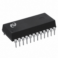
IC DAC 12BIT MPU 24-DIP
Manufacturer
National Semiconductor
Series
MICRO-DAC™r
Datasheet
1.DAC1210LCJ.pdf
(18 pages)
Specifications of DAC1210LCJ
Settling Time
1µs
Number Of Bits
12
Data Interface
Parallel
Number Of Converters
1
Voltage Supply Source
Single Supply
Power Dissipation (max)
500mW
Operating Temperature
-40°C ~ 85°C
Mounting Type
Through Hole
Package / Case
*
Case
DIP-24L
Lead Free Status / RoHS Status
Contains lead / RoHS non-compliant
Other names
*DAC1210LCJ
Available stocks
Company
Part Number
Manufacturer
Quantity
Price
Company:

Part Number:
DAC1210LCJ
Manufacturer:
NS
Quantity:
960
Company:
Part Number:
DAC1210LCJ
Manufacturer:
NS
Quantity:
960
Part Number:
DAC1210LCJ
Manufacturer:
NS/国半
Quantity:
20 000
Company:
Part Number:
DAC1210LCJ-1
Manufacturer:
NS
Quantity:
2 067


Application Hints
2 2 1 Zero and Full-Scale Adjustments
To calibrate the bipolar output circuit three adjustments are
required The first step is to set all of the digital inputs LOW
(to force I
setting the voltage at its inverting input (pin 2) to zero volts
Next with a code of all zeros still applied adjust ‘‘
scale adjust’’ the reference voltage for V
eal
opposite that of the applied reference Finally set all of the
digital inputs HIGH and adjust ‘‘
l
The polarity of the output voltage at this time will be
OUT1
to 0) then null the V
V
OUT
V
Composite Amplifier for Good DC Characteristics and Fast Output Response
OUT
e
e
Combines the low V
low V
bias current of the
LM11 with the fast
response of the LF351
Settling time
for a zero to full-
scale transition
(Continued)
b
V
4096
REF
V
REF
OS
D
2047
2048
a
drift and low
full-scale adjust’’ for
1
OS
a
8 S
R
OUT
R2
of amplifier 1 by
Fb
OS
a
e
R2
R1
g
High Voltage Power DAC
l
V
REF
b
full-
id-
14
The polarity of the output will be the same as that of the
reference voltage
3 0 APPLICATION IDEAS
In this section the digital input word is represented by the
letter D and is equal to the decimal equivalent of the 12-bit
binary input Hence D can be any integer value between 0
and 4095
TL H 5690 – 17
Related parts for DAC1210LCJ
Image
Part Number
Description
Manufacturer
Datasheet
Request
R

Part Number:
Description:
12-bit, Up Compatible, Double-buffered D To A Converters
Manufacturer:
National Semiconductor Corporation
Datasheet:

Part Number:
Description:
National Semiconductor [8-Bit D/A Converter]
Manufacturer:
National Semiconductor
Datasheet:
Part Number:
Description:
National Semiconductor [Media Coprocessor]
Manufacturer:
National Semiconductor
Datasheet:
Part Number:
Description:
Digitally Controlled Tone and Volume Circuit with Stereo Audio Power Amplifier, Microphone Preamp Stage and National 3D Sound
Manufacturer:
National Semiconductor
Datasheet:
Part Number:
Description:
Digitally Controlled Tone and Volume Circuit with Stereo Audio Power Amplifier, Microphone Preamp Stage and National 3D Sound
Manufacturer:
National Semiconductor
Datasheet:
Part Number:
Description:
AC97 Rev 2 Codec with Sample Rate Conversion and National 3D Sound
Manufacturer:
National Semiconductor
Part Number:
Description:
Manufacturer:
National Semiconductor
Datasheet:
Part Number:
Description:
Manufacturer:
National Semiconductor
Datasheet:
Part Number:
Description:
General Purpose, Low Voltage, Low Power, Rail-to-Rail Output Operational Amplifiers
Manufacturer:
National Semiconductor
Datasheet:
Part Number:
Description:
8-bit 20 MSPS flash A/D converter.
Manufacturer:
National Semiconductor
Datasheet:
Part Number:
Description:
Low Noise Quad Operational Amplifier
Manufacturer:
National Semiconductor
Datasheet:
Part Number:
Description:
Quad Differential Line Receivers
Manufacturer:
National Semiconductor
Datasheet:
Part Number:
Description:
Quad High Speed Trapezoidal? Bus Transceiver
Manufacturer:
National Semiconductor
Datasheet:
Part Number:
Description:
Dual Line Receiver
Manufacturer:
National Semiconductor
Datasheet: