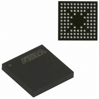
EPM240GM100C5N Altera, EPM240GM100C5N Datasheet - Page 69

EPM240GM100C5N
Manufacturer Part Number
EPM240GM100C5N
Description
IC MAX II CPLD 240 LE 100-MBGA
Manufacturer
Altera
Series
MAX® IIr
Datasheets
1.EPM240GT100C5N.pdf
(6 pages)
2.EPM240GT100C5N.pdf
(88 pages)
3.EPM240GM100C5N.pdf
(10 pages)
Specifications of EPM240GM100C5N
Programmable Type
In System Programmable
Delay Time Tpd(1) Max
4.7ns
Voltage Supply - Internal
1.71 V ~ 1.89 V
Number Of Logic Elements/blocks
240
Number Of Macrocells
192
Number Of I /o
80
Operating Temperature
0°C ~ 85°C
Mounting Type
Surface Mount
Package / Case
100-MBGA
Voltage
1.8V
Memory Type
FLASH
Number Of Logic Elements/cells
240
Family Name
MAX II
# Macrocells
192
Frequency (max)
1.8797GHz
Propagation Delay Time
7.5ns
Number Of Logic Blocks/elements
24
# I/os (max)
80
Operating Supply Voltage (typ)
1.8V
In System Programmable
Yes
Operating Supply Voltage (min)
1.71V
Operating Supply Voltage (max)
1.89V
Operating Temp Range
0C to 85C
Operating Temperature Classification
Commercial
Mounting
Surface Mount
Pin Count
100
Package Type
MBGA
Lead Free Status / RoHS Status
Lead free / RoHS Compliant
Features
-
Lead Free Status / Rohs Status
Compliant
Other names
544-1726
Available stocks
Company
Part Number
Manufacturer
Quantity
Price
Company:
Part Number:
EPM240GM100C5N
Manufacturer:
CYPESS
Quantity:
1
Company:
Part Number:
EPM240GM100C5N
Manufacturer:
ALTERA10
Quantity:
1 287
Part Number:
EPM240GM100C5N
Manufacturer:
ALTERA/阿尔特拉
Quantity:
20 000
Chapter 5: DC and Switching Characteristics
Timing Model and Specifications
Internal Timing Parameters
Table 5–15. LE Internal Timing Microparameters
© August 2009 Altera Corporation
Symbol
t
t
t
t
t
t
t
t
t
LUT
COM B
CLR
PRE
SU
H
CO
CLK HL
C
LE combinational
LUT delay
Combinational
path delay
LE register clear
delay
LE register preset
delay
LE register setup
time before clock
LE register hold
time after clock
LE register clock-
to-output delay
Minimum clock
high or low time
Register control
delay
f
Parameter
Internal timing parameters are specified on a speed grade basis independent of device
density.
microparameters for logic elements (LEs), input/output elements (IOEs), UFM
blocks, and MultiTrack interconnects. The timing values for –3, –4, and –5 speed
grades shown in
target, while –6, –7, and –8 speed grade values are based on an EPM570Z device
target.
For more explanations and descriptions about each internal timing microparameters
symbol, refer to the
Device Handbook.
Min
238
238
208
166
–3 Speed
—
—
—
—
0
Table 5–15
Grade
Max Min
571
147
235
857
—
—
—
—
—
MAX II / MAX IIG
Table 5–15
309
309
271
216
—
—
—
—
through
–4 Speed
0
Understanding Timing in MAX II Devices
Grade
1,114
Max
742
192
305
—
—
—
—
—
Table 5–22
through
Min
381
381
333
266
—
—
—
—
–5 Speed
0
Grade
1,372
Table 5–22
Max
914
236
376
—
—
—
—
—
describe the MAX II device internal timing
Min
401
401
260
253
—
—
—
—
–6 Speed
0
Grade
are based on an EPM1270 device
1,215
1,356
Max
243
380
—
—
—
—
—
Min
541
541
319
335
—
—
—
—
–7 Speed
0
MAX IIZ
Grade
chapter in the MAX II
2,247
1,722
Max
305
489
—
—
—
—
—
MAX II Device Handbook
Min
545
545
321
339
—
—
—
—
0
–8 Speed
Grade
2,247
1,741
Max
309
494
—
—
—
—
—
Unit
5–11
ps
ps
ps
ps
ps
ps
ps
ps
ps


