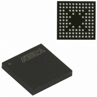
EPM570ZM100C7N Altera, EPM570ZM100C7N Datasheet - Page 43

EPM570ZM100C7N
Manufacturer Part Number
EPM570ZM100C7N
Description
IC MAX IIZ CPLD 570 LE 100-MBGA
Manufacturer
Altera
Series
MAX® IIr
Specifications of EPM570ZM100C7N
Programmable Type
In System Programmable
Delay Time Tpd(1) Max
9.0ns
Voltage Supply - Internal
1.71 V ~ 1.89 V
Number Of Logic Elements/blocks
570
Number Of Macrocells
440
Number Of I /o
76
Operating Temperature
0°C ~ 85°C
Mounting Type
Surface Mount
Package / Case
100-MBGA
Voltage
1.8V
Memory Type
FLASH
Number Of Logic Elements/cells
570
Lead Free Status / RoHS Status
Lead free / RoHS Compliant
Features
-
Other names
544-2450
Available stocks
Company
Part Number
Manufacturer
Quantity
Price
Part Number:
EPM570ZM100C7N
Manufacturer:
ALTERA/阿尔特拉
Quantity:
20 000
Introduction
IEEE Std. 1149.1 (JTAG) Boundary-Scan Support
Table 3–1. MAX II JTAG Instructions (Part 1 of 2)
© October 2008 Altera Corporation
MII51003-1.6
SAMPLE/PRELOAD
EXTEST
BYPASS
USERCODE
IDCODE
HIGHZ
JTAG Instruction
(1)
(1)
This chapter discusses how to use the IEEE Standard 1149.1 Boundary-Scan Test (BST)
circuitry in MAX II devices and includes the following sections:
■
■
All MAX
circuitry that complies with the IEEE Std. 1149.1-2001 specification. JTAG boundary-
scan testing can only be performed at any time after V
been fully powered and a t
use the JTAG port for in-system programming together with either the Quartus
software or hardware using Programming Object Files (.pof), JamTM Standard Test
and Programming Language (STAPL) Files (.jam), or Jam Byte-Code Files (.jbc).
The JTAG pins support 1.5-V, 1.8-V, 2.5-V, or 3.3-V I/O standards. The supported
voltage level and standard are determined by the V
The dedicated JTAG pins reside in Bank 1 of all MAX II devices.
MAX II devices support the JTAG instructions shown in
“IEEE Std. 1149.1 (JTAG) Boundary-Scan Support” on page 3–1
“In System Programmability” on page 3–4
00 0000 0101
00 0000 1111
11 1111 1111
00 0000 0111
00 0000 0110
00 0000 1011
Instruction Code
®
II devices provide Joint Test Action Group (JTAG) boundary-scan test (BST)
3. JTAG and In-System Programmability
CONFIG
Allows a snapshot of signals at the device pins to be captured and
examined during normal device operation, and permits an initial data
pattern to be output at the device pins.
Allows the external circuitry and board-level interconnects to be
tested by forcing a test pattern at the output pins and capturing test
results at the input pins.
Places the 1-bit bypass register between the TDI and TDO pins,
which allows the BST data to pass synchronously through selected
devices to adjacent devices during normal device operation.
Selects the 32-bit USERCODE register and places it between the
TDI and TDO pins, allowing the USERCODE to be serially shifted
out of TDO. This register defaults to all 1’s if not specified in the
Quartus II software.
Selects the IDCODE register and places it between TDI and TDO,
allowing the IDCODE to be serially shifted out of TDO.
Places the 1-bit bypass register between the TDI and TDO pins,
which allows the boundary scan test data to pass synchronously
through selected devices to adjacent devices during normal device
operation, while tri-stating all of the I/O pins.
amount of time has passed. MAX II devices can also
Description
CCIO
CCINT
of the bank where it resides.
Table
and all V
3–1.
CCIO
MAX II Device Handbook
banks have
®
II


