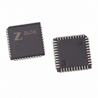
Z8927320VSG Zilog, Z8927320VSG Datasheet - Page 2

Z8927320VSG
Manufacturer Part Number
Z8927320VSG
Description
DSP 20MHZ 16-BIT W/ A/D 44-PLCC
Manufacturer
Zilog
Series
Z892x3r
Type
Fixed Pointr
Datasheet
1.Z8937320FSC00TR.pdf
(60 pages)
Specifications of Z8927320VSG
Interface
SPI, 3-Wire Serial
Clock Rate
20MHz
Non-volatile Memory
OTP (16 kB)
On-chip Ram
1kB
Voltage - I/o
5.00V
Voltage - Core
5.00V
Operating Temperature
0°C ~ 70°C
Mounting Type
Surface Mount
Package / Case
44-LCC (J-Lead)
Lead Free Status / RoHS Status
Lead free / RoHS Compliant
Available stocks
Company
Part Number
Manufacturer
Quantity
Price
Company:
Part Number:
Z8927320VSG
Manufacturer:
Zilog
Quantity:
50
GENERAL DESCRIPTION (Continued)
Z89223/273/323/373
16-Bit Digital Signal Processors with A/D Converter
OTP version of the Z89223/323, is ideal for prototypes and
early production builds.
Throughout this specification, references to the Z893x3 de-
vice apply equally to the Z89223/273/323/373, unless oth-
erwise specified.
2
RESET
AGND
HALT
CLKO
AV
CLKI
LPF
V
V
SS
CC
DD
Program
Control
Locked
Phase
Loop
Unit
ROM/OTP
16
16
Program
24
8192x16
Accumulator
16
16
24
X
Multiplier
24
24
Switch
Shifter
ALU
Bank
16
P
Figure 1. Z892X3/3x3 Functional Block Diagram
24
MUX
16 MSB
Y
16 MSB
24
Unit0
Addr
16
Gen
Data RAM0
16
D0:0–3:0
256x16
8
8
P0:0
P1:0
P2:0
DDATA
16 MSB
16
Stack
16-Bit Counter
16-Bit Counter
16-Bit Counter
Unit1
Notes: All signals with an overline are active Low. For
Power connections follow conventional descriptions:
Addr
Gen
Timer, PWM
Timer, PWM
Connection
Power
Ground
Data RAM1
16
D0:1–3:1
256x16
Timer
8
SPI
8
P0:1
P1:1
P2:1
example, in RD/WR, RD is active High and WR is
active Low. For I/O ports, P1.3 denotes Port1 bit 3. Pins
called NC are “No Connection”—they do not connect
any power, grounds, or signals.
16
Circuit
V
GND
Port 0
Port 1
Port 2
CC
Peripheral
4 Outputs
8-Bit
Interface
A/D
8-Bit I/O
8-Bit I/O
4 Inputs
16-Bit
DS000202-DSP0599
AN1
AN2
P1.2 or SDI
P1.3 or SDO
P2.2 or TMO0
P2.3 or TMO1
EA2–EA0
ED15–ED0
DS
WAIT
RD/WR
VAHI
AN0
AN3
VALO
P1.0 or INT2
P1.1 or CLKOUT
P1.4 or SS
P1.5 or SCLK
P1.6 or UI0
P1.7 or UI1
P2.0 or INT0
P2.1 or INT1
P2.4 or WAIT
P2.5 or UI2
P2.6 or TMO2
P2.7
P3.7–P3.4
P3.3–P3.0
Device
V
V
DD
SS
ZiLOG


