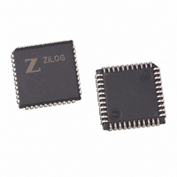
Z8927320VSG Zilog, Z8927320VSG Datasheet - Page 46

Z8927320VSG
Manufacturer Part Number
Z8927320VSG
Description
DSP 20MHZ 16-BIT W/ A/D 44-PLCC
Manufacturer
Zilog
Series
Z892x3r
Type
Fixed Pointr
Datasheet
1.Z8937320FSC00TR.pdf
(60 pages)
Specifications of Z8927320VSG
Interface
SPI, 3-Wire Serial
Clock Rate
20MHz
Non-volatile Memory
OTP (16 kB)
On-chip Ram
1kB
Voltage - I/o
5.00V
Voltage - Core
5.00V
Operating Temperature
0°C ~ 70°C
Mounting Type
Surface Mount
Package / Case
44-LCC (J-Lead)
Lead Free Status / RoHS Status
Lead free / RoHS Compliant
Available stocks
Company
Part Number
Manufacturer
Quantity
Price
Company:
Part Number:
Z8927320VSG
Manufacturer:
Zilog
Quantity:
50
SERIAL PERIPHERAL INTERFACE (Continued)
Z89223/273/323/373
16-Bit Digital Signal Processors with A/D Converter
Slave Mode Operation
SS must be asserted to enable a data transfer. Incoming data
on the SDI pin is shifted into the SPI Shift Register one data
bit per SCLK cycle. When a byte of data is received, the
SPI Shift Register contents are automatically copied into
RxBUF. The Receive Byte Available flag is set, and if en-
abled, an SPI interrupt is generated. The next byte of data
may be received at this time. The current byte in RxBUF
must be read before the next byte’s reception is complete,
or the Receive Byte Overrun flag will set, and the data in
46
INT
Counter
Interrupt
SPI
C/T0
SPI Clock
System
Clock
(from PLL Block)
SPI Receive Buffer (RxBuf)
Figure 41. SPI Block Diagram
SPI Control (SCON)
SPI Shift Register
RxBUF will be overwritten. The Receive Byte Available
flag is reset when RxBUF is read.
Unless the SPI output, SDO, is disabled, for every bit that
is transferred into the slave through the SDI pin, a bit is
transferred out through the SDO pin on the opposite clock
edge. During slave operation, SCLK is an input.
Note: Slave Mode is not available on the 44-pin package.
SPI•
I/O
DS000202-DSP0599
SDO/P1.3
SDI/P1.2
SS/P1.4
SCLK/P1.5
ZiLOG


