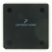
DSP56301AG80 Freescale Semiconductor, DSP56301AG80 Datasheet - Page 10

DSP56301AG80
Manufacturer Part Number
DSP56301AG80
Description
IC DSP 24BIT 80MHZ GP 208-LQFP
Manufacturer
Freescale Semiconductor
Series
DSP563xxr
Type
Fixed Pointr
Specifications of DSP56301AG80
Interface
Host Interface, SSI, SCI
Clock Rate
80MHz
Non-volatile Memory
ROM (9 kB)
On-chip Ram
24kB
Voltage - I/o
3.30V
Voltage - Core
3.30V
Operating Temperature
-40°C ~ 100°C
Mounting Type
Surface Mount
Package / Case
208-LQFP
Lead Free Status / RoHS Status
Lead free / RoHS Compliant
Available stocks
Company
Part Number
Manufacturer
Quantity
Price
Company:
Part Number:
DSP56301AG80
Manufacturer:
CONEXANT
Quantity:
4 200
Company:
Part Number:
DSP56301AG80
Manufacturer:
FREESCALE
Quantity:
7
Company:
Part Number:
DSP56301AG80
Manufacturer:
Freescale Semiconductor
Quantity:
10 000
Company:
Part Number:
DSP56301AG80B1
Manufacturer:
Freescale Semiconductor
Quantity:
10 000
Signals/Connections
1.5 External Memory Expansion Port (Port A)
Note: When the DSP56301 enters a low-power stand-by mode (Stop or Wait), it releases bus mastership and tri-
1.5.1
1.5.2
1-6
PINIT/NMI
A[0–23]
D[0–23]
Signal Name
Signal Name
Signal Name
states the relevant Port A signals:
BCLK
occur and then returns to the Wait mode.
External Address Bus
External Data Bus
. If hardware refresh of external DRAM is enabled, Port A exits the Wait mode to allow the refresh to
Input
Output
Input/Output
Type
Type
Type
Table 1-5.
Tri-stated
Tri-stated
Input
State During
State During
State During
Table 1-6.
Table 1-7.
Reset
Reset
Reset
DSP56301 Technical Data, Rev. 10
A[0–23]
Phase Lock Loop Signals (Continued)
External Address Bus Signals
,
PLL Initial/Non-Maskable Interrupt
During assertion of RESET, the value of PINIT/NMI is written into the PLL
Enable (PEN) bit of the PLL control register, determining whether the PLL is
enabled or disabled. After RESET deassertion and during normal instruction
processing, the PINIT/NMI Schmitt-trigger input is a negative-edge-triggered
Non-Maskable Interrupt (NMI) request internally synchronized to CLKOUT.
PINIT/NMI can tolerate 5 V.
D[0–23]
Address Bus
When the DSP is the bus master, A[0–23] specify the address for external
program and data memory accesses. Otherwise, the signals are tri-stated. To
minimize power dissipation, A[0–23] do not change state when external
memory spaces are not being accessed.
Data Bus
When the DSP is the bus master, D[0–23] provide the bidirectional data bus
for external program and data memory accesses. Otherwise, D[0–23] are tri-
stated.
External Data Bus Signals
,
AA0/RAS0
–
AA3/RAS3
Signal Description
Signal Description
Signal Description
,
RD
,
WR
,
BB
Freescale Semiconductor
,
CAS
,
BCLK
, and


