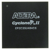
EP2C35U484C6 Altera, EP2C35U484C6 Datasheet - Page 4

EP2C35U484C6
Manufacturer Part Number
EP2C35U484C6
Description
IC CYCLONE II FPGA 33K 484-UBGA
Manufacturer
Altera
Series
Cyclone® IIr
Datasheet
1.EP2C5T144C8N.pdf
(168 pages)
Specifications of EP2C35U484C6
Number Of Logic Elements/cells
33216
Number Of Labs/clbs
2076
Total Ram Bits
483840
Number Of I /o
322
Voltage - Supply
1.15 V ~ 1.25 V
Mounting Type
Surface Mount
Operating Temperature
0°C ~ 85°C
Package / Case
484-UBGA
For Use With
P0301 - DE2 CALL FOR ACADEMIC PRICING544-1733 - PCI KIT W/CYCLONE II EP2C35N
Lead Free Status / RoHS Status
Contains lead / RoHS non-compliant
Number Of Gates
-
Other names
544-2112
Available stocks
Company
Part Number
Manufacturer
Quantity
Price
Company:
Part Number:
EP2C35U484C6
Manufacturer:
ALTERA10
Quantity:
65
Part Number:
EP2C35U484C6
Manufacturer:
ALTERA/阿尔特拉
Quantity:
20 000
Company:
Part Number:
EP2C35U484C6N
Manufacturer:
ALTERA
Quantity:
171
Features
Features
1–2
Cyclone II Device Handbook, Volume 1
■
■
■
Cyclone II devices include a powerful FPGA feature set optimized for
low-cost applications including a wide range of density, memory,
embedded multiplier, and packaging options. Cyclone II devices support
a wide range of common external memory interfaces and I/O protocols
required in low-cost applications. Parameterizable IP cores from Altera
and partners make using Cyclone II interfaces and protocols fast and easy.
The Cyclone II device family offers the following features:
■
■
■
DSP intellectual property (IP) cores
DSP Builder interface to The Mathworks Simulink and Matlab
design environment
DSP Development Kit, Cyclone II Edition
High-density architecture with 4,608 to 68,416 LEs
●
●
●
●
●
●
●
Embedded multipliers
●
●
Advanced I/O support
●
●
●
●
M4K embedded memory blocks
Up to 1.1 Mbits of RAM available without reducing available
logic
4,096 memory bits per block (4,608 bits per block including 512
parity bits)
Variable port configurations of ×1, ×2, ×4, ×8, ×9, ×16, ×18, ×32,
and ×36
True dual-port (one read and one write, two reads, or two
writes) operation for ×1, ×2, ×4, ×8, ×9, ×16, and ×18 modes
Byte enables for data input masking during writes
Up to 260-MHz operation
Up to 150 18- × 18-bit multipliers are each configurable as two
independent 9- × 9-bit multipliers with up to 250-MHz
performance
Optional input and output registers
High-speed differential I/O standard support, including LVDS,
RSDS, mini-LVDS, LVPECL, differential HSTL, and differential
SSTL
Single-ended I/O standard support, including 2.5-V and 1.8-V,
SSTL class I and II, 1.8-V and 1.5-V HSTL class I and II, 3.3-V PCI
and PCI-X 1.0, 3.3-, 2.5-, 1.8-, and 1.5-V LVCMOS, and 3.3-, 2.5-,
and 1.8-V LVTTL
Peripheral Component Interconnect Special Interest Group (PCI
SIG) PCI Local Bus Specification, Revision 3.0 compliance for 3.3-V
operation at 33 or 66 MHz for 32- or 64-bit interfaces
PCI Express with an external TI PHY and an Altera PCI Express
×1 Megacore
®
function
Altera Corporation
February 2008


