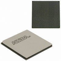
EP1AGX90EF1152C6N Altera, EP1AGX90EF1152C6N Datasheet - Page 102

EP1AGX90EF1152C6N
Manufacturer Part Number
EP1AGX90EF1152C6N
Description
IC ARRIA GX FPGA 90K 1152FBGA
Manufacturer
Altera
Series
Arria GXr
Datasheet
1.EP1AGX20CF484C6N.pdf
(234 pages)
Specifications of EP1AGX90EF1152C6N
Number Of Logic Elements/cells
90220
Number Of Labs/clbs
4511
Total Ram Bits
4477824
Number Of I /o
538
Voltage - Supply
1.15 V ~ 1.25 V
Mounting Type
Surface Mount
Operating Temperature
0°C ~ 85°C
Package / Case
1152-FBGA
Lead Free Status / RoHS Status
Lead free / RoHS Compliant
Number Of Gates
-
Other names
544-2379
Available stocks
Company
Part Number
Manufacturer
Quantity
Price
Company:
Part Number:
EP1AGX90EF1152C6N
Manufacturer:
ALTERA
Quantity:
3 000
- Current page: 102 of 234
- Download datasheet (4Mb)
2–96
Table 2–26. On-Chip Termination Support by I/O Banks
Arria GX Device Handbook, Volume 1
Series termination
Differential termination
Note to
(1) Clock pins CLK1 and CLK3, and pins FPLL[7..8]CLK do not support differential on-chip termination. Clock pins CLK0 and
On-Chip Termination Support
CLK2, do support differential on-chip termination. Clock pins in the top and bottom banks (CLK[4..7, 12..15]) do not
support differential on-chip termination.
Table
2–26:
f
f
Arria GX devices provide two types of termination:
■
■
Table 2–26
On-Chip Differential Termination (R
Arria GX devices support internal differential termination with a nominal resistance
value of 100 for LVDS input receiver buffers. LVPECL input signals (supported on
clock pins only) require an external termination resistor. R
the full range of supported differential data rates as shown in the High-Speed I/O
Specifications section of the
For more information about R
with DPA in Arria GX Devices
For more information about tolerance specifications for R
Switching Characteristics
(1)
On-chip differential termination (R
On-chip series termination (R
I/O Standard Support
SSTL-2 class I and II
1.8-V HSTL class II
lists the Arria GX OCT support per I/O bank.
1.8-V HSTL class I
1.5-V HSTL class I
SSTL-18 class II
SSTL-18 class I
HyperTransport
3.3-V LVCMOS
2.5-V LVCMOS
1.8-V LVCMOS
1.5-V LVCMOS
3.3-V LVTTL
2.5-V LVTTL
1.8-V LVTTL
1.5-V LVTTL
1.2-V HSTL
technology
LVDS
chapter.
DC & Switching Characteristics
chapter.
D
OCT, refer to the
Top and Bottom Banks
S
OCT)
D
(3, 4, 7, 8)
OCT)
D
OCT)
v
v
v
v
v
v
v
v
v
v
v
v
v
v
v
—
—
High-Speed Differential I/O Interfaces
chapter.
D
© December 2009 Altera Corporation
Left Bank (1, 2)
D
OCT, refer to the
OCT is supported across
Chapter 2: Arria GX Architecture
v
v
v
v
v
v
v
v
v
—
v
—
v
—
v
v
v
DC &
I/O Structure
Related parts for EP1AGX90EF1152C6N
Image
Part Number
Description
Manufacturer
Datasheet
Request
R

Part Number:
Description:
CYCLONE II STARTER KIT EP2C20N
Manufacturer:
Altera
Datasheet:

Part Number:
Description:
CPLD, EP610 Family, ECMOS Process, 300 Gates, 16 Macro Cells, 16 Reg., 16 User I/Os, 5V Supply, 35 Speed Grade, 24DIP
Manufacturer:
Altera Corporation
Datasheet:

Part Number:
Description:
CPLD, EP610 Family, ECMOS Process, 300 Gates, 16 Macro Cells, 16 Reg., 16 User I/Os, 5V Supply, 15 Speed Grade, 24DIP
Manufacturer:
Altera Corporation
Datasheet:

Part Number:
Description:
Manufacturer:
Altera Corporation
Datasheet:

Part Number:
Description:
CPLD, EP610 Family, ECMOS Process, 300 Gates, 16 Macro Cells, 16 Reg., 16 User I/Os, 5V Supply, 30 Speed Grade, 24DIP
Manufacturer:
Altera Corporation
Datasheet:

Part Number:
Description:
High-performance, low-power erasable programmable logic devices with 8 macrocells, 10ns
Manufacturer:
Altera Corporation
Datasheet:

Part Number:
Description:
High-performance, low-power erasable programmable logic devices with 8 macrocells, 7ns
Manufacturer:
Altera Corporation
Datasheet:

Part Number:
Description:
Classic EPLD
Manufacturer:
Altera Corporation
Datasheet:

Part Number:
Description:
High-performance, low-power erasable programmable logic devices with 8 macrocells, 10ns
Manufacturer:
Altera Corporation
Datasheet:

Part Number:
Description:
Manufacturer:
Altera Corporation
Datasheet:

Part Number:
Description:
Manufacturer:
Altera Corporation
Datasheet:

Part Number:
Description:
Manufacturer:
Altera Corporation
Datasheet:

Part Number:
Description:
CPLD, EP610 Family, ECMOS Process, 300 Gates, 16 Macro Cells, 16 Reg., 16 User I/Os, 5V Supply, 25 Speed Grade, 24DIP
Manufacturer:
Altera Corporation
Datasheet:


