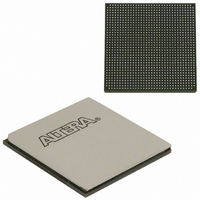
EP1AGX90EF1152C6N Altera, EP1AGX90EF1152C6N Datasheet - Page 218

EP1AGX90EF1152C6N
Manufacturer Part Number
EP1AGX90EF1152C6N
Description
IC ARRIA GX FPGA 90K 1152FBGA
Manufacturer
Altera
Series
Arria GXr
Datasheet
1.EP1AGX20CF484C6N.pdf
(234 pages)
Specifications of EP1AGX90EF1152C6N
Number Of Logic Elements/cells
90220
Number Of Labs/clbs
4511
Total Ram Bits
4477824
Number Of I /o
538
Voltage - Supply
1.15 V ~ 1.25 V
Mounting Type
Surface Mount
Operating Temperature
0°C ~ 85°C
Package / Case
1152-FBGA
Lead Free Status / RoHS Status
Lead free / RoHS Compliant
Number Of Gates
-
Other names
544-2379
Available stocks
Company
Part Number
Manufacturer
Quantity
Price
Company:
Part Number:
EP1AGX90EF1152C6N
Manufacturer:
ALTERA
Quantity:
3 000
- Current page: 218 of 234
- Download datasheet (4Mb)
4–96
DCD Measurement Techniques
Figure 4–11. DCD Measurement Technique for Non-DDIO (Single-Data Rate) Outputs
Arria GX Device Handbook, Volume 1
Figure 4–10. Duty Cycle Distortion
DCD expressed in absolution derivation, for example, D1 or D2 in
clock-period independent. DCD can also be expressed as a percentage, and the
percentage number is clock-period dependent. DCD as a percentage is defined as:
DCD is measured at an FPGA output pin driven by registers inside the corresponding
I/O element (IOE) block. When the output is a single data rate signal (non-DDIO),
only one edge of the register input clock (positive or negative) triggers output
transitions
caused by the clock input buffer or different input I/O standard does not transfer to
the output signal.
However, when the output is a double data rate input/output (DDIO) signal, both
edges of the input clock signal (positive and negative) trigger output transitions
(Figure
affect the output DCD.
(T/2 – D1) / T (the low percentage boundary)
(T/2 + D2) / T (the high percentage boundary)
4–12). Therefore, any distortion on the input clock and the input clock buffer
(Figure
4–11). Therefore, any DCD present on the input clock signal or
CLKH = T/2
Falling Edge A
Ideal Falling Edge
Clock Period (T)
D1
D2
Falling Edge B
CLKL = T/2
Chapter 4: DC and Switching Characteristics
© December 2009 Altera Corporation
Figure
Duty Cycle Distortion
4–10, is
Related parts for EP1AGX90EF1152C6N
Image
Part Number
Description
Manufacturer
Datasheet
Request
R

Part Number:
Description:
CYCLONE II STARTER KIT EP2C20N
Manufacturer:
Altera
Datasheet:

Part Number:
Description:
CPLD, EP610 Family, ECMOS Process, 300 Gates, 16 Macro Cells, 16 Reg., 16 User I/Os, 5V Supply, 35 Speed Grade, 24DIP
Manufacturer:
Altera Corporation
Datasheet:

Part Number:
Description:
CPLD, EP610 Family, ECMOS Process, 300 Gates, 16 Macro Cells, 16 Reg., 16 User I/Os, 5V Supply, 15 Speed Grade, 24DIP
Manufacturer:
Altera Corporation
Datasheet:

Part Number:
Description:
Manufacturer:
Altera Corporation
Datasheet:

Part Number:
Description:
CPLD, EP610 Family, ECMOS Process, 300 Gates, 16 Macro Cells, 16 Reg., 16 User I/Os, 5V Supply, 30 Speed Grade, 24DIP
Manufacturer:
Altera Corporation
Datasheet:

Part Number:
Description:
High-performance, low-power erasable programmable logic devices with 8 macrocells, 10ns
Manufacturer:
Altera Corporation
Datasheet:

Part Number:
Description:
High-performance, low-power erasable programmable logic devices with 8 macrocells, 7ns
Manufacturer:
Altera Corporation
Datasheet:

Part Number:
Description:
Classic EPLD
Manufacturer:
Altera Corporation
Datasheet:

Part Number:
Description:
High-performance, low-power erasable programmable logic devices with 8 macrocells, 10ns
Manufacturer:
Altera Corporation
Datasheet:

Part Number:
Description:
Manufacturer:
Altera Corporation
Datasheet:

Part Number:
Description:
Manufacturer:
Altera Corporation
Datasheet:

Part Number:
Description:
Manufacturer:
Altera Corporation
Datasheet:

Part Number:
Description:
CPLD, EP610 Family, ECMOS Process, 300 Gates, 16 Macro Cells, 16 Reg., 16 User I/Os, 5V Supply, 25 Speed Grade, 24DIP
Manufacturer:
Altera Corporation
Datasheet:


