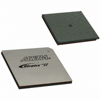
EP2S180F1508C3 Altera, EP2S180F1508C3 Datasheet - Page 223

EP2S180F1508C3
Manufacturer Part Number
EP2S180F1508C3
Description
IC STRATIX II FPGA 180K 1508FBGA
Manufacturer
Altera
Series
Stratix® IIr
Datasheet
1.EP2S15F484I4N.pdf
(238 pages)
Specifications of EP2S180F1508C3
Number Of Logic Elements/cells
179400
Number Of Labs/clbs
8970
Total Ram Bits
9383040
Number Of I /o
1170
Voltage - Supply
1.15 V ~ 1.25 V
Mounting Type
Surface Mount
Operating Temperature
0°C ~ 85°C
Package / Case
1508-FBGA
Family Name
Stratix II
Number Of Logic Blocks/elements
179400
# I/os (max)
1170
Frequency (max)
778.82MHz
Process Technology
90nm (CMOS)
Operating Supply Voltage (typ)
1.2V
Logic Cells
179400
Ram Bits
9383040
Operating Supply Voltage (min)
1.15V
Operating Supply Voltage (max)
1.25V
Operating Temp Range
0C to 85C
Operating Temperature Classification
Commercial
Mounting
Surface Mount
Pin Count
1508
Package Type
FC-FBGA
For Use With
544-1701 - DSP PRO KIT W/SII EP2S180N
Lead Free Status / RoHS Status
Contains lead / RoHS non-compliant
Number Of Gates
-
Lead Free Status / Rohs Status
Not Compliant
Other names
544-2164
Available stocks
Company
Part Number
Manufacturer
Quantity
Price
Company:
Part Number:
EP2S180F1508C3
Manufacturer:
ALTERA
Quantity:
3 000
Company:
Part Number:
EP2S180F1508C3N
Manufacturer:
ALTERA
Quantity:
624
Part Number:
EP2S180F1508C3N
Manufacturer:
ALTERA/阿尔特拉
Quantity:
20 000
High-Speed I/O
Specifications
Altera Corporation
April 2011
t
f
J
W
t
t
Timing unit interval (TUI)
f
f
Channel-to-channel skew (TCCS)
Sampling window (SW)
Input jitter
Output jitter
t
t
f
f
C
H S C L K
R I S E
F A L L
H S D R
H S D R D P A
DUTY
L O C K
H S C L K
H S C L K
Table 5–88. High-Speed Timing Specifications & Definitions
High-Speed Timing Specifications
Table 5–89. High-Speed I/O Specifications for -3 Speed Grade (Part 1 of 2)
(clock frequency)
= f
Symbol
H S D R
/ W
W = 2 to 32 (LVDS, HyperTransport technology)
(3)
W = 1 (SERDES bypass, LVDS only)
W = 1 (SERDES used, LVDS only)
Table 5–88
Table 5–89
grade Stratix II devices.
High-speed receiver/transmitter input and output clock period.
High-speed receiver/transmitter input and output clock frequency.
Deserialization factor (width of parallel data bus).
PLL multiplication factor.
Low-to-high transmission time.
High-to-low transmission time.
The timing budget allowed for skew, propagation delays, and data
sampling window. (TUI = 1/(Receiver Input Clock Frequency ×
Multiplication Factor) = t
Maximum/minimum LVDS data transfer rate (f
Maximum/minimum LVDS data transfer rate (f
The timing difference between the fastest and slowest output edges,
including t
measurement.
The period of time during which the data must be valid in order to capture
it correctly. The setup and hold times determine the ideal strobe position
within the sampling window.
Peak-to-peak input jitter on high-speed PLLs.
Peak-to-peak output jitter on high-speed PLLs.
Duty cycle on high-speed transmitter output clock.
Lock time for high-speed transmitter and receiver PLLs.
provides high-speed timing specifications definitions.
shows the high-speed I/O timing specifications for -3 speed
Conditions
C O
variation and clock skew. The clock is included in the TCCS
C
/w).
Definitions
Stratix II Device Handbook, Volume 1
DC & Switching Characteristics
Min
150
16
16
-3 Speed Grade
Notes
H S D R
H S D R D PA
Typ
= 1/TUI), non-DPA.
(1),
Max
520
500
717
= 1/TUI), DPA.
(2)
MHz
MHz
MHz
Unit
5–87


