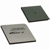
EP2S180F1508C3 Altera, EP2S180F1508C3 Datasheet - Page 92

EP2S180F1508C3
Manufacturer Part Number
EP2S180F1508C3
Description
IC STRATIX II FPGA 180K 1508FBGA
Manufacturer
Altera
Series
Stratix® IIr
Datasheet
1.EP2S15F484I4N.pdf
(238 pages)
Specifications of EP2S180F1508C3
Number Of Logic Elements/cells
179400
Number Of Labs/clbs
8970
Total Ram Bits
9383040
Number Of I /o
1170
Voltage - Supply
1.15 V ~ 1.25 V
Mounting Type
Surface Mount
Operating Temperature
0°C ~ 85°C
Package / Case
1508-FBGA
Family Name
Stratix II
Number Of Logic Blocks/elements
179400
# I/os (max)
1170
Frequency (max)
778.82MHz
Process Technology
90nm (CMOS)
Operating Supply Voltage (typ)
1.2V
Logic Cells
179400
Ram Bits
9383040
Operating Supply Voltage (min)
1.15V
Operating Supply Voltage (max)
1.25V
Operating Temp Range
0C to 85C
Operating Temperature Classification
Commercial
Mounting
Surface Mount
Pin Count
1508
Package Type
FC-FBGA
For Use With
544-1701 - DSP PRO KIT W/SII EP2S180N
Lead Free Status / RoHS Status
Contains lead / RoHS non-compliant
Number Of Gates
-
Lead Free Status / Rohs Status
Not Compliant
Other names
544-2164
Available stocks
Company
Part Number
Manufacturer
Quantity
Price
Company:
Part Number:
EP2S180F1508C3
Manufacturer:
ALTERA
Quantity:
3 000
Company:
Part Number:
EP2S180F1508C3N
Manufacturer:
ALTERA
Quantity:
624
Part Number:
EP2S180F1508C3N
Manufacturer:
ALTERA/阿尔特拉
Quantity:
20 000
I/O Structure
2–84
Stratix II Device Handbook, Volume 1
Table 2–15
strength control.
Open-Drain Output
Stratix II devices provide an optional open-drain (equivalent to an open-
collector) output for each I/O pin. This open-drain output enables the
device to provide system-level control signals (e.g., interrupt and write-
enable signals) that can be asserted by any of several devices.
Bus Hold
Each Stratix II device I/O pin provides an optional bus-hold feature. The
bus-hold circuitry can weakly hold the signal on an I/O pin at its
last-driven state. Since the bus-hold feature holds the last-driven state of
the pin until the next input signal is present, you do not need an external
pull-up or pull-down resistor to hold a signal level when the bus is
tri-stated.
Note to
(1)
3.3-V LVTTL
3.3-V LVCMOS
2.5-V LVTTL/LVCMOS
1.8-V LVTTL/LVCMOS
1.5-V LVCMOS
SSTL-2 Class I
SSTL-2 Class II
SSTL-18 Class I
SSTL-18 Class II
HSTL-18 Class I
HSTL-18 Class II
HSTL-15 Class I
HSTL-15 Class II
Table 2–15. Programmable Drive Strength
The Quartus II software default current setting is the maximum setting for each
I/O standard.
I/O Standard
Table
shows the possible settings for the I/O standards with drive
2–15:
I
Setting (mA) for Column
OH
24, 20, 16, 12, 8, 4
24, 20, 16, 12, 8, 4
/ I
12, 10, 8, 6, 4, 2
OL
12, 10, 8, 6, 4
12, 10, 8, 6, 4
12, 10, 8, 6, 4
20, 18, 16, 8
16, 12, 8, 4
20, 18, 16
20, 18, 16
24, 20, 16
Current Strength
8, 6, 4, 2
I/O Pins
12, 8
Note (1)
I
Setting (mA) for Row I/O
OH
/ I
OL
12, 10, 8, 6, 4
Altera Corporation
10, 8, 6, 4
Current Strength
8, 6, 4, 2
12, 8, 4
12, 8, 4
8, 6, 4
12, 8
Pins
8, 4
4, 2
16
-
-
-
May 2007


