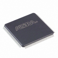
EPF10K10TC144-4N Altera, EPF10K10TC144-4N Datasheet - Page 10
EPF10K10TC144-4N
Manufacturer Part Number
EPF10K10TC144-4N
Description
IC FLEX 10K FPGA 10K 144-TQFP
Manufacturer
Altera
Series
FLEX-10K®r
Datasheet
1.EPF10K10ATC100-3.pdf
(128 pages)
Specifications of EPF10K10TC144-4N
Number Of Logic Elements/cells
576
Number Of Labs/clbs
72
Total Ram Bits
6144
Number Of I /o
102
Number Of Gates
31000
Voltage - Supply
4.75 V ~ 5.25 V
Mounting Type
Surface Mount
Operating Temperature
0°C ~ 85°C
Package / Case
144-TQFP, 144-VQFP
Family Name
FLEX 10K
Number Of Usable Gates
10000
Number Of Logic Blocks/elements
576
# I/os (max)
102
Frequency (max)
125MHz
Process Technology
CMOS
Operating Supply Voltage (typ)
5V
Logic Cells
576
Ram Bits
6144
Device System Gates
31000
Operating Supply Voltage (min)
4.75V
Operating Supply Voltage (max)
5.25V
Operating Temp Range
0C to 70C
Operating Temperature Classification
Commercial
Mounting
Surface Mount
Pin Count
144
Package Type
TQFP
Lead Free Status / RoHS Status
Lead free / RoHS Compliant
Other names
544-2202
Available stocks
Company
Part Number
Manufacturer
Quantity
Price
Company:

Part Number:
EPF10K10TC144-4N
Manufacturer:
CYPRESS
Quantity:
4 700
Company:
Part Number:
EPF10K10TC144-4N
Manufacturer:
ALTERA31
Quantity:
3 195
Part Number:
EPF10K10TC144-4N
Manufacturer:
ALTERA/阿尔特拉
Quantity:
20 000


FLEX 10K Embedded Programmable Logic Device Family Data Sheet
Logic functions are implemented by programming the EAB with a read-
only pattern during configuration, creating a large LUT. With LUTs,
combinatorial functions are implemented by looking up the results, rather
than by computing them. This implementation of combinatorial functions
can be faster than using algorithms implemented in general logic, a
performance advantage that is further enhanced by the fast access times
of EABs. The large capacity of EABs enables designers to implement
complex functions in one logic level without the routing delays associated
with linked LEs or field-programmable gate array (FPGA) RAM blocks.
For example, a single EAB can implement a 4 4 multiplier with eight
inputs and eight outputs. Parameterized functions such as LPM functions
can automatically take advantage of the EAB.
The EAB provides advantages over FPGAs, which implement on-board
RAM as arrays of small, distributed RAM blocks. These FPGA RAM
blocks contain delays that are less predictable as the size of the RAM
increases. In addition, FPGA RAM blocks are prone to routing problems
because small blocks of RAM must be connected together to make larger
blocks. In contrast, EABs can be used to implement large, dedicated blocks
of RAM that eliminate these timing and routing concerns.
EABs can be used to implement synchronous RAM, which is easier to use
than asynchronous RAM. A circuit using asynchronous RAM must
generate the RAM write enable (WE) signal, while ensuring that its data
and address signals meet setup and hold time specifications relative to the
WE signal. In contrast, the EAB’s synchronous RAM generates its own WE
signal and is self-timed with respect to the global clock. A circuit using the
EAB’s self-timed RAM need only meet the setup and hold time
specifications of the global clock.
When used as RAM, each EAB can be configured in any of the following
sizes: 256 8, 512
4, 1,024 2, or 2,048
1. See
Figure
2.
Figure 2. EAB Memory Configurations
2,048 1
256
8
512
4
1,024 2
10
Altera Corporation
Related parts for EPF10K10TC144-4N
Image
Part Number
Description
Manufacturer
Datasheet
Request
R

Part Number:
Description:
CYCLONE II STARTER KIT EP2C20N
Manufacturer:
Altera
Datasheet:


Part Number:
Description:
CPLD, EP610 Family, ECMOS Process, 300 Gates, 16 Macro Cells, 16 Reg., 16 User I/Os, 5V Supply, 35 Speed Grade, 24DIP
Manufacturer:
Altera Corporation
Datasheet:
Part Number:
Description:
CPLD, EP610 Family, ECMOS Process, 300 Gates, 16 Macro Cells, 16 Reg., 16 User I/Os, 5V Supply, 15 Speed Grade, 24DIP
Manufacturer:
Altera Corporation
Datasheet:
Part Number:
Description:
Manufacturer:
Altera Corporation
Datasheet:
Part Number:
Description:
CPLD, EP610 Family, ECMOS Process, 300 Gates, 16 Macro Cells, 16 Reg., 16 User I/Os, 5V Supply, 30 Speed Grade, 24DIP
Manufacturer:
Altera Corporation
Datasheet:
Part Number:
Description:
High-performance, low-power erasable programmable logic devices with 8 macrocells, 10ns
Manufacturer:
Altera Corporation
Datasheet:
Part Number:
Description:
High-performance, low-power erasable programmable logic devices with 8 macrocells, 7ns
Manufacturer:
Altera Corporation
Datasheet:
Part Number:
Description:
Classic EPLD
Manufacturer:
Altera Corporation
Datasheet:
Part Number:
Description:
High-performance, low-power erasable programmable logic devices with 8 macrocells, 10ns
Manufacturer:
Altera Corporation
Datasheet:
Part Number:
Description:
Manufacturer:
Altera Corporation
Datasheet:
Part Number:
Description:
Manufacturer:
Altera Corporation
Datasheet:
Part Number:
Description:
Manufacturer:
Altera Corporation
Datasheet:
Part Number:
Description:
CPLD, EP610 Family, ECMOS Process, 300 Gates, 16 Macro Cells, 16 Reg., 16 User I/Os, 5V Supply, 25 Speed Grade, 24DIP
Manufacturer:
Altera Corporation
Datasheet: