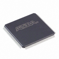
EPF10K10TC144-4N Altera, EPF10K10TC144-4N Datasheet - Page 29

EPF10K10TC144-4N
Manufacturer Part Number
EPF10K10TC144-4N
Description
IC FLEX 10K FPGA 10K 144-TQFP
Manufacturer
Altera
Series
FLEX-10K®r
Datasheet
1.EPF10K10ATC100-3.pdf
(128 pages)
Specifications of EPF10K10TC144-4N
Number Of Logic Elements/cells
576
Number Of Labs/clbs
72
Total Ram Bits
6144
Number Of I /o
102
Number Of Gates
31000
Voltage - Supply
4.75 V ~ 5.25 V
Mounting Type
Surface Mount
Operating Temperature
0°C ~ 85°C
Package / Case
144-TQFP, 144-VQFP
Family Name
FLEX 10K
Number Of Usable Gates
10000
Number Of Logic Blocks/elements
576
# I/os (max)
102
Frequency (max)
125MHz
Process Technology
CMOS
Operating Supply Voltage (typ)
5V
Logic Cells
576
Ram Bits
6144
Device System Gates
31000
Operating Supply Voltage (min)
4.75V
Operating Supply Voltage (max)
5.25V
Operating Temp Range
0C to 70C
Operating Temperature Classification
Commercial
Mounting
Surface Mount
Pin Count
144
Package Type
TQFP
Lead Free Status / RoHS Status
Lead free / RoHS Compliant
Other names
544-2202
Available stocks
Company
Part Number
Manufacturer
Quantity
Price
Company:
Part Number:
EPF10K10TC144-4N
Manufacturer:
CYPRESS
Quantity:
4 700
Company:
Part Number:
EPF10K10TC144-4N
Manufacturer:
ALTERA31
Quantity:
3 195
Part Number:
EPF10K10TC144-4N
Manufacturer:
ALTERA/阿尔特拉
Quantity:
20 000
FLEX 10K Embedded Programmable Logic Device Family Data Sheet
I/O Element
An I/O element (IOE) contains a bidirectional I/O buffer and a register
that can be used either as an input register for external data that requires
a fast setup time, or as an output register for data that requires fast clock-
to-output performance. In some cases, using an LE register for an input
register will result in a faster setup time than using an IOE register. IOEs
can be used as input, output, or bidirectional pins. For bidirectional
registered I/O implementation, the output register should be in the IOE
and, the data input and output enable register should be LE registers
placed adjacent to the bidirectional pin. The Compiler uses the
programmable inversion option to invert signals from the row and
column interconnect automatically where appropriate.
Figure 13
shows
the bidirectional I/O registers.
Altera Corporation
29


