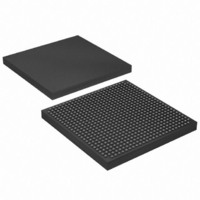
EP1S25F672C8 Altera, EP1S25F672C8 Datasheet - Page 233

EP1S25F672C8
Manufacturer Part Number
EP1S25F672C8
Description
IC STRATIX FPGA 25K LE 672-FBGA
Manufacturer
Altera
Series
Stratix®r
Datasheet
1.EP1S10F780C7.pdf
(276 pages)
Specifications of EP1S25F672C8
Number Of Logic Elements/cells
25660
Number Of Labs/clbs
2566
Total Ram Bits
1944576
Number Of I /o
473
Voltage - Supply
1.425 V ~ 1.575 V
Mounting Type
Surface Mount
Operating Temperature
0°C ~ 85°C
Package / Case
672-FBGA
Lead Free Status / RoHS Status
Contains lead / RoHS non-compliant
Number Of Gates
-
Other names
544-1119
Available stocks
Company
Part Number
Manufacturer
Quantity
Price
Company:
Part Number:
EP1S25F672C8
Manufacturer:
AD
Quantity:
2 562
Company:
Part Number:
EP1S25F672C8
Manufacturer:
ALTERA
Quantity:
3 000
Part Number:
EP1S25F672C8
Manufacturer:
ALTERA
Quantity:
20 000
Company:
Part Number:
EP1S25F672C8N
Manufacturer:
ALTERA
Quantity:
465
Part Number:
EP1S25F672C8N
Manufacturer:
ALTERA/阿尔特拉
Quantity:
20 000
- Current page: 233 of 276
- Download datasheet (4Mb)
Altera Corporation
January 2006
Notes to
(1)
(2)
(3)
(4)
3.3-V SSTL-3 Class I
2.5-V SSTL-2 Class II
2.5-V SSTL-2 Class I
1.8-V SSTL-18 Class II
1.8-V SSTL-18 Class I
1.5-V HSTL Class II
1.5-V HSTL Class I
1.8-V HSTL Class II
1.8-V HSTL Class I
3.3-V PCI
3.3-V PCI-X 1.0
3.3-V Compact PCI
3.3-V AGP 1X
3.3-V CTT
Table 4–101. Reporting Methodology For Maximum Timing For Single-Ended Output Pins (Part 2 of 2)
Notes
Input measurement point at internal node is 0.5 × V
Output measuring point for data is V
Input stimulus edge rate is 0 to V
The first value is for output rising edge and the second value is for output falling edge. The hyphen (-) indicates
infinite resistance or disconnection.
I/O Standard
(1), (2),
Table
(4)
(4)
4–101:
(3)
(4)
(4)
–/25
–/25
–/25
–/25
R
Ω
–
–
–
–
–
–
–
–
–
–
UP
CCINT
25/–
25/–
25/–
25/–
R
Ω
MEAS
–
–
–
–
–
–
–
–
–
–
DN
in 0.5 ns (internal signal) from the driver preceding the IO buffer.
.
Loading and Termination
R
25
25
25
25
25
25
Ω
0
0
0
0
0
0
0
0
S
CCINT
50
25
50
25
50
25
50
25
50
50
R
.
Ω
–
–
–
–
T
2.950
2.370
2.370
1.650
1.650
1.400
1.400
1.650
1.650
2.950
2.950
2.950
2.950
2.050
V
(V)
CCIO
Stratix Device Handbook, Volume 1
DC & Switching Characteristics
1.250
1.110
1.110
0.760
0.760
0.700
0.700
0.700
0.700
2.950
2.950
2.950
2.950
1.350
VTT
(V)
(pF)
30
30
30
30
30
20
20
20
20
10
10
10
10
30
C
L
Measurement
0.841/1.814
0.841/1.814
0.841/1.814
0.841/1.814
V
1.250
1.110
1.110
0.760
0.760
0.680
0.680
0.880
0.880
1.350
Point
MEAS
4–63
Related parts for EP1S25F672C8
Image
Part Number
Description
Manufacturer
Datasheet
Request
R

Part Number:
Description:
CYCLONE II STARTER KIT EP2C20N
Manufacturer:
Altera
Datasheet:

Part Number:
Description:
CPLD, EP610 Family, ECMOS Process, 300 Gates, 16 Macro Cells, 16 Reg., 16 User I/Os, 5V Supply, 35 Speed Grade, 24DIP
Manufacturer:
Altera Corporation
Datasheet:

Part Number:
Description:
CPLD, EP610 Family, ECMOS Process, 300 Gates, 16 Macro Cells, 16 Reg., 16 User I/Os, 5V Supply, 15 Speed Grade, 24DIP
Manufacturer:
Altera Corporation
Datasheet:

Part Number:
Description:
Manufacturer:
Altera Corporation
Datasheet:

Part Number:
Description:
CPLD, EP610 Family, ECMOS Process, 300 Gates, 16 Macro Cells, 16 Reg., 16 User I/Os, 5V Supply, 30 Speed Grade, 24DIP
Manufacturer:
Altera Corporation
Datasheet:

Part Number:
Description:
High-performance, low-power erasable programmable logic devices with 8 macrocells, 10ns
Manufacturer:
Altera Corporation
Datasheet:

Part Number:
Description:
High-performance, low-power erasable programmable logic devices with 8 macrocells, 7ns
Manufacturer:
Altera Corporation
Datasheet:

Part Number:
Description:
Classic EPLD
Manufacturer:
Altera Corporation
Datasheet:

Part Number:
Description:
High-performance, low-power erasable programmable logic devices with 8 macrocells, 10ns
Manufacturer:
Altera Corporation
Datasheet:

Part Number:
Description:
Manufacturer:
Altera Corporation
Datasheet:

Part Number:
Description:
Manufacturer:
Altera Corporation
Datasheet:

Part Number:
Description:
Manufacturer:
Altera Corporation
Datasheet:

Part Number:
Description:
CPLD, EP610 Family, ECMOS Process, 300 Gates, 16 Macro Cells, 16 Reg., 16 User I/Os, 5V Supply, 25 Speed Grade, 24DIP
Manufacturer:
Altera Corporation
Datasheet:


