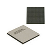
EP4SGX530HH35C2N Altera, EP4SGX530HH35C2N Datasheet - Page 54

EP4SGX530HH35C2N
Manufacturer Part Number
EP4SGX530HH35C2N
Description
IC STRATIX IV FPGA 530K 1152HBGA
Manufacturer
Altera
Series
Stratix® IV GXr
Datasheets
1.EP4SGX110DF29C3N.pdf
(80 pages)
2.EP4SGX110DF29C3N.pdf
(1154 pages)
3.EP4SGX110DF29C3N.pdf
(432 pages)
4.EP4SGX110DF29C3N.pdf
(22 pages)
5.EP4SGX110DF29C3N.pdf
(30 pages)
6.EP4SGX110DF29C3N.pdf
(72 pages)
7.EP4SGX530HH35C2N.pdf
(1145 pages)
Specifications of EP4SGX530HH35C2N
Number Of Logic Elements/cells
531200
Number Of Labs/clbs
21248
Total Ram Bits
27376
Number Of I /o
564
Voltage - Supply
0.87 V ~ 0.93 V
Mounting Type
Surface Mount
Operating Temperature
0°C ~ 85°C
Package / Case
1152-HBGA
Family Name
Stratix® IV
Number Of Logic Blocks/elements
531200
# Registers
424960
# I/os (max)
560
Process Technology
40nm
Operating Supply Voltage (typ)
900mV
Logic Cells
531200
Ram Bits
28033024
Operating Supply Voltage (min)
0.87V
Operating Supply Voltage (max)
0.93V
Operating Temp Range
0C to 85C
Operating Temperature Classification
Commercial
Mounting
Surface Mount
Pin Count
1152
Package Type
FCHBGA
Lead Free Status / RoHS Status
Lead free / RoHS Compliant
Number Of Gates
-
Lead Free Status / Rohs Status
Compliant
Available stocks
Company
Part Number
Manufacturer
Quantity
Price
1–46
Table 1–34. PLL Specifications for Stratix IV Devices (Part 2 of 2)—Preliminary
Stratix IV Device Handbook Volume 4: Device Datasheet and Addendum
t
t
t
t
f
Notes to
(1) This specification is limited in the Quartus II software by the I/O maximum frequency. The maximum I/O frequency is different for each I/O
(2) The VCO frequency reported by the Quartus II software in the PLL summary section of the compilation report takes into consideration the VCO
(3) This specification is limited by the lower of the two: I/O F
(4) A high input jitter directly affects the PLL output jitter. To have low PLL output clock jitter, you must provide a clean clock source that is less
(5) F
(6) Peak-to-peak jitter with a probability level of 10
(7) The cascaded PLL specification is only applicable with the following condition:
(8) High bandwidth PLL settings are not supported in external feedback mode.
(9) External memory interface clock output jitter specifications use a different measurement method, which is available in
OUTCCJ_DC
OUTPJ_IO
(9)
OUTCCJ_IO
(9)
CASC_OUTPJ_DC
(6),
DRIFT
Symbol
standard.
post-scale counter K value. Therefore, if the counter K has a value of 2, the frequency reported can be lower than the f
than 120 ps.
to the intrinsic jitter of the PLL, when an input jitter of 30 ps is applied. The external memory interface clock output jitter specifications use a
different measurement method and are available in
A. Upstream PLL: 0.59Mhz ≤ Upstream PLL BW < 1 MHz
B. Downstream PLL: Downstream PLL BW > 2 MHz
page
REF
(7)
Table
is fIN/N when N = 1.
1–60.
(6),
(6),
(6)
1–34:
Cycle to Cycle Jitter for dedicated clock output
(F
Cycle to Cycle Jitter for dedicated clock output
(F
Period Jitter for clock output on regular I/O
(F
Period Jitter for clock output on regular I/O
(F
Cycle to Cycle Jitter for clock output on regular I/O
(F
Cycle to Cycle Jitter for clock output on regular I/O
(F
Period Jitter for dedicated clock output in cascaded PLLs
(F
Period Jitter for dedicated clock output in cascaded PLLs
(F
Frequency drift after PFDENA is disabled for duration of
100 us
OUT
OUT
OUT
OUT
OUT
OUT
OUT
OUT
≥ 100 MHz)
< 100 MHz)
< 100 MHz)
< 100 MHz)
< 100MHz)
≥ 100 MHz)
≥ 100 MHz)
≥100MHz)
Parameter
–12
(14 sigma, 99.99999999974404% confidence level). The output jitter specification applies
Table 1–50 on page
MAX
or F
OUT
of the PLL.
1–61.
Chapter 1: DC and Switching Characteristics for Stratix IV Devices
Min
—
—
—
—
—
—
—
—
—
Typ
—
—
—
—
—
—
—
—
—
April 2011 Altera Corporation
Max
17.5
175
600
600
250
±10
60
60
25
Switching Characteristics
VCO
Table 1–48 on
specification.
mUI (p-p)
mUI (p-p)
mUI (p-p)
mUI (p-p)
ps (p-p)
ps (p-p)
ps (p-p)
ps (p-p)
Unit
%


