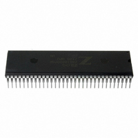
Z8S18020PSG Zilog, Z8S18020PSG Datasheet - Page 67

Z8S18020PSG
Manufacturer Part Number
Z8S18020PSG
Description
IC Z180 MPU 64-DIP
Manufacturer
Zilog
Datasheet
1.Z8S18010PSG.pdf
(71 pages)
Specifications of Z8S18020PSG
Processor Type
Z180
Features
Enhanced Z180
Speed
20MHz
Voltage
5V
Mounting Type
Through Hole
Package / Case
64-DIP (0.750", 19.05mm)
Processor Series
Z8S180X
Core
Z80
Data Bus Width
8 bit
Maximum Clock Frequency
20 MHz
Number Of Timers
2
Operating Supply Voltage
0 V to 3.3 V
Maximum Operating Temperature
+ 70 C
Mounting Style
Through Hole
Development Tools By Supplier
Z8S18000ZEM
Minimum Operating Temperature
0 C
Lead Free Status / RoHS Status
Lead free / RoHS Compliant
Other names
269-4301
Z8S18020PSG
Z8S18020PSG
Available stocks
Company
Part Number
Manufacturer
Quantity
Price
Company:
Part Number:
Z8S18020PSG
Manufacturer:
Zilog
Quantity:
201
ZiLOG
dress (on 4-KB boundaries) for Common Area 1. This con-
dition also determines the most recent address of the Bank
Area. All bits of
The Z8S180/Z8L180 is descended from two different an-
cestor processors, ZiLOG’s original Z80 and the Hitachi
64180. The Operating Mode Control Register (
be programmed to select between certain differences be-
tween the Z80 and the 64180.
A
0
–A
18
MREQ
D
0
(A
–D
RD
M1
ST
19
7
)
are set to
T
1
T
2
PC
specifies the start (Low) ad-
1
EDH
T
during
3
T
1
T
2
.
4DH
T
3
) can
PC+1
T
I
T
(on 4-KB boundaries) for the Bank Area. This condition
also determines the most recent address of Common Area
0
set to a
When
opcode fetch cycle, the
first machine cycle of the
On the Z8S180/Z8L180, this choice makes the processor
fetch one
wait-state memory, the processor uses three clock machine
cycles that are not fully Z80-timing-compatible.
When
ing instruction fetch cycles. After fetching one
tion with normal timing, the processor returns and refetches
the instruction using Z80-compatible cycles that drive
Low. This timing compatibility may be required by external
Z80 peripherals to properly decode the
I
. All bits of
T
I
1
T
1
during reset.
instruction. When fetching a
0
1
T
, the processor does not drive
, the
2
are set to
T
EDH
This bit controls the
3
PC
output is asserted Low during the
T
specifies the start (Low) address
1
I
acknowledge cycle, and the
during
acknowledge.
T
1
T
2
PC+1
4DH
T
3
.
output and is
instruction.
from zero-
T
Low dur-
I
instruc-


