MPC8248VRMIBA Freescale Semiconductor, MPC8248VRMIBA Datasheet - Page 14
MPC8248VRMIBA
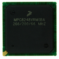
Manufacturer Part Number
MPC8248VRMIBA
Description
IC MPU POWERQUICC II 516-PBGA
Manufacturer
Freescale Semiconductor
Datasheet
1.MPC8248VRMIBA.pdf
(60 pages)
Specifications of MPC8248VRMIBA
Processor Type
MPC82xx PowerQUICC II 32-bit
Speed
266MHz
Voltage
1.5V
Mounting Type
Surface Mount
Package / Case
516-PBGA
For Use With
CWH-PPC-8248N-VE - KIT EVAL SYSTEM QUICCSTART 8248
Lead Free Status / RoHS Status
Lead free / RoHS Compliant
Features
-
Available stocks
Company
Part Number
Manufacturer
Quantity
Price
Company:

Part Number:
MPC8248VRMIBA
Manufacturer:
Freescale Semiconductor
Quantity:
135
Company:
Part Number:
MPC8248VRMIBA
Manufacturer:
FREESCALE
Quantity:
996
Company:
Part Number:
MPC8248VRMIBA
Manufacturer:
Freescale Semiconductor
Quantity:
10 000
Part Number:
MPC8248VRMIBA
Manufacturer:
FREESCALE
Quantity:
20 000
Part Number:
MPC8248VRMIBA266/200/66
Manufacturer:
FREESCALE
Quantity:
20 000


Thermal Characteristics
4.5
To determine the junction temperature of the device in the application after prototypes are available, the
thermal characterization parameter (Ψ
measurement of the temperature at the top center of the package case using the following equation:
where:
The thermal characterization parameter is measured per JEDEC JESD51-2 specification using a 40 gauge
type T thermocouple epoxied to the top center of the package case. The thermocouple should be positioned
so that the thermocouple junction rests on the package. A small amount of epoxy is placed over the
thermocouple junction and over 1 mm of wire extending from the junction. The thermocouple wire is
placed flat against the case to avoid measurement errors caused by cooling effects of the thermocouple
wire.
4.6
Each VDD and VDDH pin should be provided with a low-impedance path to the board’s power supplies.
Each ground pin should likewise be provided with a low-impedance path to ground. The power supply pins
drive distinct groups of logic on chip. The VDD and VDDH power supplies should be bypassed to ground
using by-pass capacitors located as close as possible to the four sides of the package. For filtering high
frequency noise, a capacitor of 0.1uF on each VDD and VDDH pin is recommended. Further, for medium
frequency noise, a total of 2 capacitors of 47uF for VDD and 2 capacitors of 47uF for VDDH are also
recommnded. The capacitor leads and associated printed circuit traces connecting to chip VDD, VDDH
and ground should be kept to less than half an inch per capacitor lead. Boards should employ separate inner
layers for power and GND planes.
All output pins on the MPC8272 have fast rise and fall times. Printed circuit (PC) trace interconnection
length should be minimized to minimize overdamped conditions and reflections caused by these fast
output switching times. This recommendation particularly applies to the address and data buses. Maximum
PC trace lengths of six inches are recommended. Capacitance calculations should consider all device loads
as well as parasitic capacitances due to the PC traces. Attention to proper PCB layout and bypassing
becomes especially critical in systems with higher capacitive loads because these loads create higher
transient currents in the VDD and GND circuits. Pull up all unused inputs or signals that will be inputs
during reset. Special care should be taken to minimize the noise levels on the PLL supply pins.
4.7
14
Semiconductor Equipment and Materials International
805 East Middlefield Rd.
Mountain View, CA 94043
MIL-SPEC and EIA/JESD (JEDEC) Specifications
(Available from Global Engineering Documents)
Ψ
T
P
D
T
JT
Experimental Determination
Layout Practices
References
= thermocouple temperature on top of package
= power dissipation in package
= thermal characterization parameter
T
J
= T
T
+ (Ψ
MPC8272 PowerQUICC II™ Family Hardware Specifications, Rev. 2
JT
× P
D
)
JT
) can be used to determine the junction temperature with a
(415) 964-5111
800-854-7179 or
303-397-7956
Freescale Semiconductor
Related parts for MPC8248VRMIBA
Image
Part Number
Description
Manufacturer
Datasheet
Request
R

Part Number:
Description:
Mpc8248 Powerquicc Ii Integrated Communications Processor
Manufacturer:
Freescale Semiconductor, Inc
Datasheet:
Part Number:
Description:
Manufacturer:
Freescale Semiconductor, Inc
Datasheet:
Part Number:
Description:
Manufacturer:
Freescale Semiconductor, Inc
Datasheet:
Part Number:
Description:
Manufacturer:
Freescale Semiconductor, Inc
Datasheet:
Part Number:
Description:
Manufacturer:
Freescale Semiconductor, Inc
Datasheet:
Part Number:
Description:
Manufacturer:
Freescale Semiconductor, Inc
Datasheet:
Part Number:
Description:
Manufacturer:
Freescale Semiconductor, Inc
Datasheet:
Part Number:
Description:
Manufacturer:
Freescale Semiconductor, Inc
Datasheet:
Part Number:
Description:
Manufacturer:
Freescale Semiconductor, Inc
Datasheet:
Part Number:
Description:
Manufacturer:
Freescale Semiconductor, Inc
Datasheet:
Part Number:
Description:
Manufacturer:
Freescale Semiconductor, Inc
Datasheet:
Part Number:
Description:
Manufacturer:
Freescale Semiconductor, Inc
Datasheet:
Part Number:
Description:
Manufacturer:
Freescale Semiconductor, Inc
Datasheet:
Part Number:
Description:
Manufacturer:
Freescale Semiconductor, Inc
Datasheet:
Part Number:
Description:
Manufacturer:
Freescale Semiconductor, Inc
Datasheet: