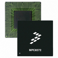
MPC8272CVRMIBA Freescale Semiconductor, MPC8272CVRMIBA Datasheet - Page 59

MPC8272CVRMIBA
Manufacturer Part Number
MPC8272CVRMIBA
Description
IC MPU POWERQUICC II 516-PBGA
Manufacturer
Freescale Semiconductor
Specifications of MPC8272CVRMIBA
Processor Type
MPC82xx PowerQUICC II 32-bit
Speed
266MHz
Voltage
1.5V
Mounting Type
Surface Mount
Package / Case
516-PBGA
Lead Free Status / RoHS Status
Lead free / RoHS Compliant
Features
-
Available stocks
Company
Part Number
Manufacturer
Quantity
Price
Company:
Part Number:
MPC8272CVRMIBA
Manufacturer:
Freescale Semiconductor
Quantity:
135
Company:
Part Number:
MPC8272CVRMIBA
Manufacturer:
Freescale Semiconductor
Quantity:
10 000
Part Number:
MPC8272CVRMIBA
Manufacturer:
N/A
Quantity:
20 000
Freescale Semiconductor
Revision
0.2
0.1
0
12/2003
9/2003
5/2003
Date
•
•
•
•
•
•
•
•
• Sections 4.1–4.5 and 4.7 on thermal characteristics: New
•
• Addition of “Note: Temperature Reflow for the VR Package" on page 55
•
•
•
•
• Addition of the MPC8271 and the MPC8247 (these devices do not have a security engine)
•
•
• Modification of note 1 for
•
•
• Addition of ZQ package code to
NDA release
MPC8272 PowerQUICC II™ Family Hardware Specifications, Rev. 2
Table
Table
Table
Table
Table 5
CPCI_HS_ES to PCI_REQ1 (AF14)
CPCI_HS_LED to PCI_GNT1 (AE13)
CPCI_HS_ENUM to PCI_GNT2 (AF21)
Table 5
on other PowerQUICC II devices:
PCI_CFG0 (PCI_HOST_EN) (AC21)
PCI_CFG1 (PCI_ARB_EN) (AE22)
PCI_CFG2 (DLL_ENABLE) (AE23)
PCI_PAR (AF12)
PCI_FRAME (AD15)
PCI_TRDY(AF16)
PCI_IRDY (AF15)
PCI_STOP (AE15)
DEVSEL (AE14)
PCI_IDSEL (AC17)
PCI_PERR (AD14)
PCI_SERR (AD13)
PCI_REQ0–2 (AAE20, AF14, AB14)
PCI_GNT0–2 (AD20, AE13, AF21)
PCI_RST (AF22)
PCI_INTA (AE21)
PCI_C0-3 (AE12, AF13, AC15, AE18)
PCI_AD0-31
Table 5
PCI_ARB_EN (AE22)
Table
Section 7, “Clock Configuration
PCI_MODCK is a bit in the Hard Reset Configuration Word. It is not an input signal as it is in
the MPC8280 Family and MPC8260 Family.
Table
Table
Note 4 unchanged.
Table
Table
of note 1.
Table
Table
Table
to both CS5 and GND. AD8 is only assigned to CS5.
Table
Table 22. Document Revision History (continued)
1: New
2: New
4: Modification of VDD and VCCSYN to 1.45–1.60 V
5: Addition of note 2 regarding TRST and PORESET (see V
6: Addition of R
20: Addition of note 2 to TRST (E21) and PORESET (C24)
20: Removal of Thermal0 (D19) and Thermal1(J3). These pins are now “No connects.”
20: Removal of Spare0 (AD24). This pin is now a “No connect.” Note 5 unchanged.
20: Addition of PCI_MODE (AD22). This pin was previously listed as “Ground.” Addition
5: Addition of note 2 to V
5: Changed I
20: Addition of ball AD9 to GND. In rev 0 of this document, AD8 was listed as assigned
20: Addition of note 4 to Thermal0 (D19) and Thermal1(J3)
and
and
and
Table
Table
Table
20: Modification of PCI signal names for consistency with PCI signal names
20: Addition of muxed signals
20: Corrected assertion level (added “ “) PCI_HOST_EN (AC21) and
OL
θJT
for 60x signals to 6.0 mA
and note 4
Table
IH
16,
Modes”: Modification to first paragraph. Note that
Figure 15
Substantive Changes
Table
17,
Table
18, and
Table 19
IH
row of
Document Revision History
Table
5)
59


