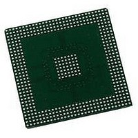
MPC5200CBV400 Freescale Semiconductor, MPC5200CBV400 Datasheet - Page 62

MPC5200CBV400
Manufacturer Part Number
MPC5200CBV400
Description
IC MPU 32BIT 400MHZ PPC 272-PBGA
Manufacturer
Freescale Semiconductor
Datasheet
1.MPC5200CVR400B.pdf
(80 pages)
Specifications of MPC5200CBV400
Processor Type
MPC52xx PowerPC 32-Bit
Speed
400MHz
Voltage
1.5V
Mounting Type
Surface Mount
Package / Case
272-PBGA
Core Size
32 Bit
No. Of I/o's
56
Ram Memory Size
16KB
Cpu Speed
400MHz
No. Of Timers
8
Embedded Interface Type
CAN, I2C, SPI, UART, USB
No. Of Pwm Channels
8
Digital Ic Case Style
BGA
Rohs Compliant
No
Family Name
MPC52xx
Device Core
PowerPC
Device Core Size
32b
Frequency (max)
400MHz
Instruction Set Architecture
RISC
Supply Voltage 1 (typ)
1.5V
Operating Supply Voltage (max)
1.58V
Operating Supply Voltage (min)
1.42V
Operating Temp Range
-40C to 85C
Operating Temperature Classification
Industrial
Mounting
Surface Mount
Pin Count
272
Package Type
BGA
Lead Free Status / RoHS Status
Contains lead / RoHS non-compliant
Features
-
Lead Free Status / Rohs Status
Not Compliant
Available stocks
Company
Part Number
Manufacturer
Quantity
Price
Company:
Part Number:
MPC5200CBV400
Manufacturer:
FREESCAL
Quantity:
200
Company:
Part Number:
MPC5200CBV400
Manufacturer:
Freescale Semiconductor
Quantity:
10 000
Company:
Part Number:
MPC5200CBV400B
Manufacturer:
FREESCAL
Quantity:
200
Electrical and Thermal Characteristics
3.3.17 IEEE 1149.1 (JTAG) AC Specifications
62
NOTES:
1
2
3
TRST is an asynchronous signal. The setup time is for test purposes only.
Non-test, other than TDI and TMS, signal input timing with respect to TCK.
Non-test, other than TDO, signal output timing with respect to TCK.
Sym
10
11
12
13
—
1
2
3
4
5
6
7
8
9
TCK frequency of operation.
TCK cycle time.
TCK clock pulse width measured at 1.5V.
TCK rise and fall times.
TRST setup time to tck falling edge
TRST assert time.
Input data setup time
Input data hold time
TCK to output data valid
TCK to output high impedance
TMS, TDI data setup time.
TMS, TDI data hold time.
TCK to TDO data valid.
TCK to TDO high impedance.
TCK
Figure 47. Timing Diagram—JTAG Clock Input
2
.
2
.
3
Characteristic
3
.
Table 51. JTAG Timing Specification
3
.
MPC5200 Data Sheet, Rev. 4
1
.
VM
3
2
VM = Midpoint Voltage
Numbers shown reference
1
VM
1.08
Min
40
10
15
0
0
5
5
0
0
5
1
0
0
2
Max
25
30
30
—
—
15
15
—
—
—
—
—
—
3
Freescale Semiconductor
Table
MHz
Unit
ns
ns
ns
ns
ns
ns
ns
ns
ns
ns
ns
ns
ns
VM
51.
SpecID
A17.10
A17.11
A17.12
A17.13
A17.14
A17.1
A17.2
A17.3
A17.4
A17.5
A17.6
A17.7
A17.8
A17.9


