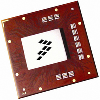
MPC8560CPX667JC Freescale Semiconductor, MPC8560CPX667JC Datasheet - Page 11

MPC8560CPX667JC
Manufacturer Part Number
MPC8560CPX667JC
Description
IC MPU PWRQUICC III 783-FCPBGA
Manufacturer
Freescale Semiconductor
Series
PowerQUICC IIIr
Specifications of MPC8560CPX667JC
Processor Type
MPC85xx PowerQUICC III 32-Bit
Speed
667MHz
Voltage
1.2V
Mounting Type
Surface Mount
Package / Case
783-FCPBGA
Core Size
32 Bit
Program Memory Size
64KB
Cpu Speed
667MHz
Embedded Interface Type
I2C, MII, SPI, TDM, UTOPIA
Digital Ic Case Style
BGA
No. Of Pins
783
Rohs Compliant
No
Family Name
MPC85XX
Device Core
PowerQUICC III
Device Core Size
32b
Frequency (max)
667MHz
Instruction Set Architecture
RISC
Supply Voltage 1 (typ)
1.2V
Operating Supply Voltage (max)
1.26V
Operating Supply Voltage (min)
1.14V
Operating Temp Range
-40C to 105C
Operating Temperature Classification
Industrial
Mounting
Surface Mount
Pin Count
783
Package Type
FCBGA
For Use With
MPC8560ADS-BGA - BOARD APPLICATION DEV 8560
Lead Free Status / RoHS Status
Contains lead / RoHS non-compliant
Features
-
Lead Free Status / Rohs Status
Not Compliant
Available stocks
Company
Part Number
Manufacturer
Quantity
Price
Company:
Part Number:
MPC8560CPX667JC
Manufacturer:
Freescale Semiconductor
Quantity:
10 000
Figure 2
The MPC8560 core voltage must always be provided at nominal 1.2 V (see
recommended core voltage). Voltage to the processor interface I/Os are provided through separate sets of
supply pins and must be provided at the voltages shown in
respect to the associated I/O supply voltage. OV
circuits and satisfy appropriate LVCMOS type specifications. The DDR SDRAM interface uses a
single-ended differential receiver referenced the externally supplied MV
GV
Freescale Semiconductor
DD
/2) as is appropriate for the SSTL2 electrical signaling standard.
shows the undershoot and overshoot voltages at the interfaces of the MPC8560.
V
V
Note:
IH
IL
t
SYS
Figure 2. Overshoot/Undershoot Voltage for GV
G/L/OV
MPC8560 Integrated Processor Hardware Specifications, Rev. 4.2
G/L/OV
refers to the clock period associated with the SYSCLK signal.
GND – 0.3 V
GND – 0.7 V
G/L/OV
DD
DD
+ 20%
+ 5%
GND
DD
DD
and LV
Not to Exceed 10%
Table
of t
DD
SYS
based receivers are simple CMOS I/O
2. The input voltage threshold scales with
1
DD
/OV
REF
DD
Table 2
signal (nominally set to
/LV
DD
for actual
Electrical Characteristics
11


