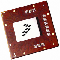
MPC8560CPX667JC Freescale Semiconductor, MPC8560CPX667JC Datasheet - Page 67

MPC8560CPX667JC
Manufacturer Part Number
MPC8560CPX667JC
Description
IC MPU PWRQUICC III 783-FCPBGA
Manufacturer
Freescale Semiconductor
Series
PowerQUICC IIIr
Specifications of MPC8560CPX667JC
Processor Type
MPC85xx PowerQUICC III 32-Bit
Speed
667MHz
Voltage
1.2V
Mounting Type
Surface Mount
Package / Case
783-FCPBGA
Core Size
32 Bit
Program Memory Size
64KB
Cpu Speed
667MHz
Embedded Interface Type
I2C, MII, SPI, TDM, UTOPIA
Digital Ic Case Style
BGA
No. Of Pins
783
Rohs Compliant
No
Family Name
MPC85XX
Device Core
PowerQUICC III
Device Core Size
32b
Frequency (max)
667MHz
Instruction Set Architecture
RISC
Supply Voltage 1 (typ)
1.2V
Operating Supply Voltage (max)
1.26V
Operating Supply Voltage (min)
1.14V
Operating Temp Range
-40C to 105C
Operating Temperature Classification
Industrial
Mounting
Surface Mount
Pin Count
783
Package Type
FCBGA
For Use With
MPC8560ADS-BGA - BOARD APPLICATION DEV 8560
Lead Free Status / RoHS Status
Contains lead / RoHS non-compliant
Features
-
Lead Free Status / Rohs Status
Not Compliant
Available stocks
Company
Part Number
Manufacturer
Quantity
Price
Company:
Part Number:
MPC8560CPX667JC
Manufacturer:
Freescale Semiconductor
Quantity:
10 000
The compliance of receiver input signals RD[0:15] and RFRAME with their minimum data valid window
(DV) specification shall be determined by generating an eye pattern for each of the data signals and
comparing the eye pattern of each data signal with the RapidIO receive mask shown in
value of X2 used to construct the mask shall be (1 – DV
±600 mV maximum input voltage values are from the DC specification. A signal is compliant with the data
valid window specification if and only if the receive mask can be positioned on the signal’s eye pattern
such that the eye pattern falls entirely within the unshaded portion of the mask.
The eye pattern for a data signal is generated by making a large number of recordings of the signal and
then overlaying the recordings. The number of recordings used to generate the eye shall be large enough
that further increasing the number of recordings used does not cause the resulting eye pattern to change
from one that complies with the RapidIO receive mask to one that does not. Each data signal in the
interface shall be carrying random or pseudo-random data when the recordings are made. If
pseudo-random data is used, the length of the pseudo-random sequence (repeat length) shall be long
Freescale Semiconductor
Duty cycle of the clock input
Data valid
Allowable static skew between any two data inputs
within a 8-/9-bit group
Allowable static skew of data inputs to associated clock
Notes:
1.Measured at V
2.Measured using the RapidIO receive mask shown in
3.See
4.See
5.Guaranteed by design.
Figure
Figure 48
49.
ID
and
Table 53. RapidIO Receiver AC Timing Specifications—1 Gbps Data Rate
= 0 V.
Characteristic
Figure
MPC8560 Integrated Processor Hardware Specifications, Rev. 4.2
49.
–100
–600
600
100
0
0
Figure 46. RapidIO Receive Mask
X2
Figure
t
SKEW,PAIR
Symbol
t
46.
DPAIR
Time (UI)
DC
DV
DV
min
)/2. The ±100 mV minimum data valid and
–200
Min
425
47
—
1–X2
Range
Max
300
200
53
—
1
Figure
Unit
ps
ps
ps
%
46. The
Notes
1, 5
RapidIO
2
3
4
67


