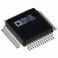
AD1836AASZ Analog Devices Inc, AD1836AASZ Datasheet - Page 12

AD1836AASZ
Manufacturer Part Number
AD1836AASZ
Description
IC CODEC 4ADC/6DAC 24 BIT 52MQFP
Manufacturer
Analog Devices Inc
Type
General Purposer
Datasheet
1.AD1836AASZ.pdf
(24 pages)
Specifications of AD1836AASZ
Data Interface
Serial
Resolution (bits)
24 b
Number Of Adcs / Dacs
4 / 6
Sigma Delta
Yes
S/n Ratio, Adcs / Dacs (db) Typ
105 / 108
Dynamic Range, Adcs / Dacs (db) Typ
105 / 108
Voltage - Supply, Analog
4.75 V ~ 5.25 V
Voltage - Supply, Digital
4.75 V ~ 5.25 V
Operating Temperature
-40°C ~ 85°C
Mounting Type
Surface Mount
Package / Case
52-BQFP
Audio Codec Type
Stereo
No. Of Adcs
4
No. Of Dacs
6
No. Of Input Channels
4
No. Of Output Channels
6
Adc / Dac Resolution
24bit
Adcs / Dacs Signal To Noise Ratio
108dB
Lead Free Status / RoHS Status
Lead free / RoHS Compliant
For Use With
AD1836AZ-DBRD - BOARD EVAL FOR AD1836AAD1836A-DBRD - BOARD EVAL FOR AD1836A
Lead Free Status / RoHS Status
Lead free / RoHS Compliant, Lead free / RoHS Compliant
Available stocks
Company
Part Number
Manufacturer
Quantity
Price
Company:
Part Number:
AD1836AASZ
Manufacturer:
Analog Devices Inc
Quantity:
10 000
Company:
Part Number:
AD1836AASZRL
Manufacturer:
Analog Devices Inc
Quantity:
10 000
AD1836A
through an FPGA or other large digital chip before being
applied to the AD1836A. In most cases, this will induce clock
jitter due to the fact that the clock signal is sharing common
power and ground connections with other unrelated digital
output signals.
The six DAC channels use a common serial bit clock to clock in
the serial data and a common left-right framing clock. The four
ADC channels output a common serial bit clock and a left-right
framing clock. The clock signals are all synchronous with the
sample rate.
RESET AND POWER-DOWN
Reset will power down the chip and set the control registers to
their default settings. After reset is de-asserted, an initialization
routine will run inside the AD1836A to clear all memories to
zero. This initialization lasts for approximately 4500 MCLKs.
The power-down bit in the DAC Control Register 1 and ADC
Control Register 1 will power down the respective digital
section. The analog circuitry does not power down. All other
register settings are retained.
To avoid possible synchronization problems, if MCLK is 512 f
or 768 f
within the first 3072 MCLK cycles after reset, or DLRCLK and
DBCLK should be withheld until after the internal initialization
completes (see above).
S
, the clock rate should be set in ADC Control Register 3
CLATCH
CDATA
COUT
CCLK
D15
D14
D9
D8
Figure 3. Format of SPI Signal
Rev. 0 | Page 12 of 24
S
SERIAL CONTROL PORT
The AD1836A has an SPI compatible control port that permits
programming the internal control registers for the ADCs and
DACs and for reading the ADC signal level from the internal
peak detectors. The DAC output levels may be independently
programmed by means of an internal digital attenuator
adjustable in 1024 linear steps.
The SPI control port is a 4-wire serial control port. The format
is similar to the Motorola SPI format except the input data-word
is 16 bits wide. The maximum serial bit clock frequency is 8 MHz
and may be completely asynchronous to the sample rate of the
ADCs and DACs. Figure 3 shows the format of the SPI signal.
All control registers are write-only. They cannot be read back.
The ADC peak registers are read-only. They are reset to zero each
time they are read and are updated at the next sample time.
Due to an anomaly in the SPI interface, when a write to a DAC
control register follows after a read or a write to an ADC
register, it may not be executed properly. Any such write should
be performed twice.
D0
D0


