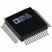
AD1836AASZ Analog Devices Inc, AD1836AASZ Datasheet - Page 13

AD1836AASZ
Manufacturer Part Number
AD1836AASZ
Description
IC CODEC 4ADC/6DAC 24 BIT 52MQFP
Manufacturer
Analog Devices Inc
Type
General Purposer
Datasheet
1.AD1836AASZ.pdf
(24 pages)
Specifications of AD1836AASZ
Data Interface
Serial
Resolution (bits)
24 b
Number Of Adcs / Dacs
4 / 6
Sigma Delta
Yes
S/n Ratio, Adcs / Dacs (db) Typ
105 / 108
Dynamic Range, Adcs / Dacs (db) Typ
105 / 108
Voltage - Supply, Analog
4.75 V ~ 5.25 V
Voltage - Supply, Digital
4.75 V ~ 5.25 V
Operating Temperature
-40°C ~ 85°C
Mounting Type
Surface Mount
Package / Case
52-BQFP
Audio Codec Type
Stereo
No. Of Adcs
4
No. Of Dacs
6
No. Of Input Channels
4
No. Of Output Channels
6
Adc / Dac Resolution
24bit
Adcs / Dacs Signal To Noise Ratio
108dB
Lead Free Status / RoHS Status
Lead free / RoHS Compliant
For Use With
AD1836AZ-DBRD - BOARD EVAL FOR AD1836AAD1836A-DBRD - BOARD EVAL FOR AD1836A
Lead Free Status / RoHS Status
Lead free / RoHS Compliant, Lead free / RoHS Compliant
Available stocks
Company
Part Number
Manufacturer
Quantity
Price
Company:
Part Number:
AD1836AASZ
Manufacturer:
Analog Devices Inc
Quantity:
10 000
Company:
Part Number:
AD1836AASZRL
Manufacturer:
Analog Devices Inc
Quantity:
10 000
POWER SUPPLY AND VOLTAGE REFERENCE
The AD1836A is designed for 5 V supplies. Separate power
supply pins are provided for the analog and digital sections.
These pins should be bypassed with 100 nF ceramic chip
capacitors, as close to the pins as possible, to minimize noise
pickup. A bulk aluminum electrolytic capacitor of at least 22 µF
should also be provided on the same PC board as the codec. For
critical applications, improved performance will be obtained
with separate supplies for the analog and digital sections. If this
is not possible, it is recommended that the analog and digital
supplies be isolated by means of a ferrite bead in series with
each supply. It is important that the analog supply be as clean as
possible.
For ease in interfacing to various logic families, the digital
output drivers are supplied from the ODVDD pin. For CMOS
logic, this should be connected to the 5 V digital supply. For
3.3 V logic, it should be connected to the 3.3 V supply. For TTL
levels, it can be tied to either. All digital inputs are compatible
with TTL and CMOS levels.
The internal voltage reference V
(FILTR) and should be bypassed as close as possible to the chip,
with a parallel combination of 10 µF and 100 nF. The reference
voltage may be used to bias external op amps to the common-
mode voltage of the input and output signal pins. The current
drawn should be limited to less than 50 µA. This source can be
connected directly to op amp inputs but should be buffered if it
is required to drive resistive networks.
The FILTD pin should be connected to an external grounded
capacitor. This pin is used to reduce the noise of the internal
DAC bias circuitry, thereby reducing the DAC output noise. In
some cases, this capacitor may be eliminated with little effect on
performance.
REF
is brought out on Pin 13
Rev. 0 | Page 13 of 24
SERIAL DATA PORTS—DATA FORMAT
The ADC serial data output mode defaults to the popular I
format, where the data is delayed by 1 BCLK interval from the
edge of the LRCLK. By programming Bits 8 and 9 in ADC
Control Register 2, the serial mode can be changed to right
justified (RJ), left justified DSP (DSP), left justified (LJ), Packed
Mode 128, or Packed Mode 256. In the RJ mode, it is necessary
to set Bits 6 and 7 to define the width of the data-word.
The DAC serial data input mode defaults to I
programming Bits 5, 6, and 7 in DAC Control Register 1, the
mode can be changed to RJ, DSP, LJ, Packed Mode 128, or
Packed Mode 256. The word width defaults to 24 bits but
can be changed by programming Bits 3 and 4 in DAC Control
Register 1. The packed modes accept six channels of data at the
DSDATA1 input pin, which is routed independently to each of
the six internal DACs.
A special “auxiliary mode” is provided to allow two external
stereo ADCs and one external stereo DAC to be interfaced with
the AD1836A to provide 8 in/8 out operation. In addition, this
mode supports glueless interface to a single SHARC DSP serial
port, allowing a SHARC DSP to access all eight channels of
analog I/O. In this special mode, many pins are redefined; see
Table 11 for a list of redefined pins. Two versions of this mode
are available. In the master mode, the AD1836A provides the
LRCLK and BCLK signals for the external ADCs and DAC. In
the slave mode, external ADC1 provides the LRCLK and BCLK
signals (which must be divided down properly from the
external master clock), and the AD1836A will sync to these
external clocks. In the absence of the external ADC clocks in
slave mode, the ALRCLK and ABCLK outputs of the AD1836A
(TDM frame sync and bit clock) will default to be the same as in
master mode. See
Figure 9 through Figure 11 for details of these modes. Figure 12
shows the internal signal flow diagram of the auxiliary mode.
The following figures show the serial mode formats.
2
S. By
AD1836A
2
S


