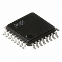
TDA8029HL/C207,118 NXP Semiconductors, TDA8029HL/C207,118 Datasheet - Page 23

TDA8029HL/C207,118
Manufacturer Part Number
TDA8029HL/C207,118
Description
IC SMART CARD READER 32-LQFP
Manufacturer
NXP Semiconductors
Datasheet
1.TDA8029HLC207118.pdf
(59 pages)
Specifications of TDA8029HL/C207,118
Package / Case
32-LQFP
Controller Type
Smart Card Reader Interface
Interface
Serial
Voltage - Supply
2.7 V ~ 6 V
Current - Supply
250mA
Operating Temperature
-40°C ~ 90°C
Mounting Type
Surface Mount
Maximum Operating Temperature
+ 90 C
Minimum Operating Temperature
- 40 C
Mounting Style
SMD/SMT
Lead Free Status / RoHS Status
Lead free / RoHS Compliant
Lead Free Status / RoHS Status
Lead free / RoHS Compliant, Lead free / RoHS Compliant
Other names
568-2233-2
935274733118
TDA8029HL07BD-T
935274733118
TDA8029HL07BD-T
Available stocks
Company
Part Number
Manufacturer
Quantity
Price
Company:
Part Number:
TDA8029HL/C207,118
Manufacturer:
NXP Semiconductors
Quantity:
10 000
Part Number:
TDA8029HL/C207,118
Manufacturer:
NXP/恩智浦
Quantity:
20 000
Philips Semiconductors
9397 750 14145
Product data sheet
8.4.3 Interrupt priority high register (IPH)
8.5 Dual DPTR
Table 29:
Table 30:
Each interrupt priority is assigned with a bit in register IP and a bit in register IPH, see
[1]
The dual DPTR structure is a way by which the TDA8029 will specify the address of an
external data memory location. There are two 16-bit DPTR registers that address the
external memory, and a single bit called DPS (bit 0 of the AUXR1 register) that allows the
program code to switch between them.
The DPS bit should be saved by software when switching between DPTR0 and DPTR1.
The GF bit (bit 2 in register AUXR1) is a general purpose user-defined flag. Note that bit 2
is not writable and is always read as a logic 0. This allows the DPS bit to be quickly
toggled simply by executing an INC AUXR1 instruction without affecting the GF or LPEP
bits.
The instructions that refer to DPTR refer to the data pointer that is currently selected using
bit 0 of the AUXR1 register. The six instructions that use the DPTR are listed in
and an illustration is given in
Table 31:
The data pointer can be accessed on a byte-by-byte basis by specifying the low or high
byte in an instruction which accesses the SFRs.
Bit
7 and 6
5
4
3
2
1
0
Instruction
INC DPTR
MOV DPTR, #data 16
MOV A, @A + DPTR
MOVX A, @DPTR
MOVX @DPTR, A
JMP @A + DPTR
Do not write logic 1s to reserved bits. These bits may be used in future 80C51 family products to invoke
new features. In that case, the reset or inactive value of the new bit will be logic 0, and its active value will
be logic 1. The value read from a reserved bit is indeterminate.
7
-
Symbol
-
PT2H
PSH
PT1H
PX1H
PT0H
PX0H
IPH - interrupt priority high register (address B7h) bit allocation
IPH - interrupt priority high register (address B7h) bit description
DPTR Instructions
6
-
Rev. 03 — 22 February 2005
PT2H
Description
Not implemented. Reserved for future use
Timer 2 interrupt priority.
Serial port interrupt prioritizes.
Timer 1 interrupt priority.
External interrupt 1 priority.
Timer 0 interrupt priority.
External interrupt 0 priority.
5
Figure
8.
PSH
4
Comment
increments the data pointer by 1
loads the DPTR with a 16-bit constant
move code byte relative to DPTR to ACC
move external RAM (16-bit address) to ACC
move ACC to external RAM (16-bit address)
jump indirect relative to DPTR
PT1H
3
Low power single card reader
© Koninklijke Philips Electronics N.V. 2005. All rights reserved.
PX1H
2
[1]
PT0H
TDA8029
1
Table
Table 31
PX0H
23 of 59
23.
0


