KSZ8873MLL Micrel Inc, KSZ8873MLL Datasheet
KSZ8873MLL
Specifications of KSZ8873MLL
Available stocks


Related parts for KSZ8873MLL

KSZ8873MLL Summary of contents
Page 1
... KSZ8873MLL/FLL/RLL also offer a by-pass mode. In this mode, the processor connected to the switch through the MII interface can be shut down without impacting the normal switch operation. ...
Page 2
... Typical – VoIP Phone – Set-top/Game Box – Automotive – Industrial Control – IPTV POF – SOHO Residential Gateway – Broadband Gateway / Firewall / VPN – Integrated DSL/Cable Modem – Wireless LAN access point + gateway – Standalone 10/100 switch 2 KSZ8873MLL/FLL/RLL +85 C M9999-081010-1.3 ...
Page 3
... Micrel, Inc. Ordering Information Part Number Temperature Range KSZ8873MLL KSZ8873MLLI –40ºC to +85ºC KSZ8873MLL AM -40 KSZ8873FLL KSZ8873FLLI –40ºC to +85ºC KSZ8873RLL KSZ8873RLLI –40ºC to +85ºC Revision History Revision Date Summary of Changes 1.0 03/25/08 Initial release 1.1 06/26/09 Combined Register Description to initial release. ...
Page 4
... Port Individual MAC address and Source Port Filtering ............................................................................................ 28 MII Interface Operation ..................................................................................................................................................... 28 RMII Interface Operation .................................................................................................................................................. 29 MII Management (MIIM) Interface .................................................................................................................................... 31 Serial Management Interface (SMI).................................................................................................................................. 31 Advanced Switch Functions .............................................................................................................................................. 32 Bypass Mode .................................................................................................................................................................... 32 IEEE 802.1Q VLAN Support............................................................................................................................................. 32 QoS Priority Support......................................................................................................................................................... 33 Port-Based Priority..................................................................................................................................................... 33 802.1p-Based Priority ................................................................................................................................................ 33 DiffServ-Based Priority .............................................................................................................................................. 34 September 2010 4 KSZ8873MLL/FLL/RLL M9999-092309-1.2 ...
Page 5
... Register 10 (0x0A): Global Control 8......................................................................................................................... 54 Register 11 (0x0B): Global Control 9......................................................................................................................... 54 Register 12 (0x0C): Global Control 10 ...................................................................................................................... 54 Register 13 (0x0D): Global Control 11 ...................................................................................................................... 54 Register 14 (0x0E): Global Control 12....................................................................................................................... 55 Register 15 (0x0F): Global Control 13....................................................................................................................... 55 Port Registers (Registers 16 – 95) ................................................................................................................................... 56 Register 16 (0x10): Port 1 Control 0.......................................................................................................................... 56 September 2010 5 KSZ8873MLL/FLL/RLL M9999-092309-1.2 ...
Page 6
... Register 99 (0x63): TOS Priority Control Register 3 ................................................................................................. 67 Register 100 (0x64): TOS Priority Control Register 4 ............................................................................................... 67 Register 101 (0x65): TOS Priority Control Register 5 ............................................................................................... 67 Register 102 (0x66): TOS Priority Control Register 6 ............................................................................................... 68 Register 103 (0x67): TOS Priority Control Register 7 ............................................................................................... 68 September 2010 6 KSZ8873MLL/FLL/RLL M9999-092309-1.2 ...
Page 7
... Register 174 (0xAE): PM Usage Flow Control Select Mode 4 .................................................................................. 76 Register 175 (0xAF): TXQ Split for Q3 in Port 1........................................................................................................ 76 Register 176 (0xB0): TXQ Split for Q2 in Port 1........................................................................................................ 76 Register 177 (0xB1): TXQ Split for Q1 in Port 1........................................................................................................ 76 Register 178 (0xB2): TXQ Split for Q0 in Port 1........................................................................................................ 76 September 2010 7 KSZ8873MLL/FLL/RLL M9999-092309-1.2 ...
Page 8
... Operating Ratings ............................................................................................................................................................ 88 (4) Electrical Characteristics ................................................................................................................................................ 88 EEPROM Timing .............................................................................................................................................................. 90 MII Timing ......................................................................................................................................................................... 91 RMII Timing....................................................................................................................................................................... Slave Mode Timing ..................................................................................................................................................... 94 SPI Timing ........................................................................................................................................................................ 96 Auto-Negotiation Timing ................................................................................................................................................... 98 MDC/MDIO Timing ........................................................................................................................................................... 99 Reset Timing................................................................................................................................................................... 100 Reset Circuit ................................................................................................................................................................... 101 Selection of Isolation Transformers................................................................................................................................ 102 Selection of Reference Crystal ........................................................................................................................................ 102 Package Information ......................................................................................................................................................... 103 September 2010 8 KSZ8873MLL/FLL/RLL M9999-092309-1.2 ...
Page 9
... Figure 24. I2C Input Timing.................................................................................................................................................. 94 Figure 25. I2C Start Bit Timing............................................................................................................................................. 94 Figure 26. I2C Stop Bit Timing ............................................................................................................................................. 94 Figure 27. I2C Output Timing............................................................................................................................................... 94 Figure 28. SPI Input Timing ................................................................................................................................................. 96 Figure 29. SPI Output Timing............................................................................................................................................... 97 Figure 30. Auto-Negotiation Timing ..................................................................................................................................... 98 Figure 31. MDC/MDIO Timing.............................................................................................................................................. 99 Figure 35. 64-Pin LQFP Package ...................................................................................................................................... 104 September 2010 9 KSZ8873MLL/FLL/RLL M9999-092309-1.2 ...
Page 10
... Table 27. SPI Input Timing Parameters............................................................................................................................... 96 Table 28. SPI Output Timing Parameters ............................................................................................................................ 97 Table 29. Auto-Negotiation Timing Parameters................................................................................................................... 98 Table 30. MDC/MDIO Timing Parameters ........................................................................................................................... 99 Table 31. Reset Timing Parameters .................................................................................................................................. 100 Table 32. Transformer Selection Criteria ........................................................................................................................... 102 Table 33. Qualified Single Port Magnetics......................................................................................................................... 102 Table 34. Typical Reference Crystal Characteristics ......................................................................................................... 102 September 2010 10 KSZ8873MLL/FLL/RLL M9999-092309-1.2 ...
Page 11
... Input in MAC MII and RMII mode. RLL: Reference clock input Note: pull up or down is needed if internal reference clock is used in RLL. Ipd Switch MII transmit error in MII mode 0= MII link indicator from host in MII PHY mode link on port 3 MII PHY mode and enable By-pass mode. 11 KSZ8873MLL/FLL/RLL M9999-092309-1.2 ...
Page 12
... Strap option: XCLK Frequency Selection MHz MHz I SPI slave mode: chip select (active low) When SPISN is high, the KSZ8873MLL/FLL/RLL is deselected and SPIQ is held in high impedance state. A high-to-low transition is used to initiate SPI data transfer. Note: an external pull-up is needed on this pin when use. 12 KSZ8873MLL/FLL/RLL M9999-092309-1 ...
Page 13
... VDDCO pin. The ferrite bead is requested between analog and digital 1.8V core power. NC Unused pin. No external connection. Ipu/O Port 1 LED Indicators: Default: Speed (refer to register 195 bit[5:4]) Strap option: Port 3 flow control selection(P3FFC always enable (force) port 3 flow control feature PD = disable 13 KSZ8873MLL/FLL/RLL M9999-092309-1.2 ...
Page 14
... SCL_MDC SDA_MDIO SPISN [P2LED1, P2LED0] = [1, 1] – SMI/MIIM-mode In SMI mode, the KSZ8873MLL/FLL/RLL provides access to all its internal 8-bit registers through its SCL_MDC and SDA_MDIO pins. In MIIM mode, the KSZ8873MLL/FLL/RLL provides access to its 16-bit MIIM registers through its SDC_MDC and SDA_MDIO pins. ...
Page 15
... Opd = Output w/ internal pull-down. September 2010 (1) Type Description Ipu/O Ipu Hardware reset pin (active low) I MLL/RLL: connect to analog ground by 1Kohm pull-down resistor. FLL: Fiber signal detect P 1.8 analog VDD input power supply from VDDCO (pin 56) through external Ferrite bead and capacitor. 15 KSZ8873MLL/FLL/RLL M9999-092309-1.2 ...
Page 16
... Micrel, Inc. Pin Configuration September 2010 64-Pin LQFP (Top View) 16 KSZ8873MLL/FLL/RLL M9999-092309-1.2 ...
Page 17
... The KSZ8873MLL/FLL/RLL contains two 10/100 physical layer transceivers and three MAC units with an integrated Layer 2 managed switch. The KSZ8873MLL/FLL/RLL has the flexibility to reside in either a managed or unmanaged design managed design, the host processor has complete control of the KSZ8873MLL/FLL/RLL via the SMI interface, MIIM interface, SPI bus, or ...
Page 18
... The auto-sense function detects remote transmit and receive pairs and correctly assigns transmit and receive pairs for the KSZ8873MLL/FLL/RLL device. This feature is extremely useful when end users are unaware of cable types, and also, saves on an additional uplink configuration connection. The auto-crossover feature can be disabled through the port control registers, or MIIM PHY registers ...
Page 19
... NIC card (MDI) and a switch, or hub (MDI-X). 10/100 Ethernet Media Dependent Interface Transmit Pair Receive Pair Modular Connector (RJ-45) September 2010 1 2 Straight 3 Cable NIC Figure 1. Typical Straight Cable Connection 19 KSZ8873MLL/FLL/RLL 10/100 Ethernet Media Dependent Interface 1 Receive Pair Transmit Pair Modular Connector (RJ-45) HUB (Repeater or Switch) M9999-092309-1.2 ...
Page 20
... Ethernet Media Dependent Interface Receive Pair Transmit Pair Modular Connector (RJ-45) (Repeater or Switch) September 2010 1 Crossover Cable HUB Figure 2. Typical Crossover Cable Connection 20 KSZ8873MLL/FLL/RLL 10/100 Ethernet Media Dependent Interface 1 Receive Pair Transmit Pair Modular Connector (RJ-45) HUB (Repeater or Switch) M9999-092309-1.2 ...
Page 21
... If auto-negotiation is not supported or the KSZ8873MLL/FLL/RLL link partner is forced to bypass auto-negotiation, the KSZ8873MLL/FLL/RLL sets its operating mode by observing the signal at its receiver. This is known as parallel detection, and allows the KSZ8873MLL/FLL/RLL to establish link by listening for a fixed signal protocol in the absence of auto-negotiation advertisement protocol. ...
Page 22
... The ‘11’ case, invalid test, occurs when the KSZ8873MLL/FLL/RLL is unable to shut down the link partner. In this instance, the test is not run, since it would be impossible for the KSZ8873MLL/FLL/RLL to determine if the detected signal is a reflection of the signal generated or a signal from another source. 5. Get distance to fault by concatenating register 42, bit [0] and register 43, bits [7:0] ...
Page 23
... The energy detect mode provides a mechanism to save more power than in the normal operation mode when the KSZ8873MLL/FLL/RLL is not connected to an active link partner. In this mode, the device will save up to 50% of the power. If the cable is not plugged, the KSZ8873MLL/FLL/RLL can automatically enter to a low power state, a.k.a., the energy detect mode ...
Page 24
... This feature can be enabled or disabled through register 3 (0x03) bit [2]. Forwarding The KSZ8873MLL/FLL/RLL forwards packets using the algorithm that is depicted in the following flowcharts. Figure 4 shows stage one of the forwarding algorithm where the search engine looks up the VLAN ID, static table, and dynamic table for the destination address, and comes up with “ ...
Page 25
... YES FOUND Search Static Table NOT FOUND FOUND Dynamic Table Search Table NOT FOUND Search complete. Get PTF1 from VLAN Table PTF1 25 KSZ8873MLL/FLL/RLL - Search VLAN table - Ingress VLAN filtering - Discard NPVID check This search is based DA+FID This search is based on DA+FID M9999-092309-1.2 ...
Page 26
... These include framing errors, Frame Check Sequence (FCS) errors, alignment errors, and illegal size packet errors. 2. IEEE802.3x PAUSE frames KSZ8873MLL/FLL/RLL intercepts these packets and performs full duplex flow control accordingly. 3. "Local" packets Based on destination address (DA) lookup. If the destination port from the lookup table matches the port from which the packet originated, the packet is defined as " ...
Page 27
... The flow control is based on availability of the system resources, including available buffers, available transmit queues and available receive queues. The KSZ8873MLL/FLL/RLL will flow control a port that has just received a packet if the destination port resource is busy. The KSZ8873MLL/FLL/RLL issues a flow control frame (XOFF), containing the maximum pause time defined by the IEEE 802 ...
Page 28
... Port Individual MAC address and Source Port Filtering The KSZ8873MLL/FLL/RLL provide individual MAC address for port 1 and port 2 respectively. They can be set at register 142-147 and 148-153. With this feature, the CPU connected to the port 3 can receive the packets from two internet subnets which has their own MAC address ...
Page 29
... MAC device. Since the switch filters error frames, these MII error signals are not used by the KSZ8873MLL/FLL. So, for PHY mode operation, if the device interfacing with the KSZ8873MLL/FLL has an MRXER input pin, it needs to be tied low. And, for MAC mode operation, if the device interfacing with the KSZ8873MLL/FLL has an MTXER input pin, it also needs to be tied low. ...
Page 30
... Receive data valid Receive data bit 1 Receive data bit 0 Transmit enable Transmit data bit 1 Transmit data bit 0 Receive error Table 7. RMII Signal Connections 30 KSZ8873MLL/FLL/RLL KSZ8873RLL RMII Signal (direction) REFCLKI_3 (input) SMRXDV3 (output) SMRXD31 (output) SMRXD30 (output) SMTXEN3 (input) SMTXD31 (input) SMTXD30 (input) ...
Page 31
... Input/Output (MDIO) Interface. This interface allows upper-layer devices to monitor and control the states of the KSZ8873MLL/FLL/RLL. An external device with MDC/MDIO capability is used to read the PHY status or configure the PHY settings. Further detail on the MIIM interface is found in Clause 22.2.4.5 of the IEEE 802.3u Specification and refer to 802 ...
Page 32
... Yes Advanced VLAN features, such as “Ingress VLAN filtering” and “Discard Non PVID packets” are also supported by the KSZ8873MLL/FLL/RLL. These features can be set on a per port basis, and are defined in register 18, 34 and 50 for ports 1, 2 and 3, respectively. September 2010 ...
Page 33
... The CRC is recalculated for both tag insertion and tag removal. 802.1p Priority Field Re-mapping is a QoS feature that allows the KSZ8873MLL/FLL/RLL to set the “User Priority Ceiling” at any ingress port. If the ingress packet’s priority field has a higher priority value than the default tag’s priority field of the ingress port, the packet’ ...
Page 34
... BPDU packets). The “overriding” bit is set so that the switch forwards those specific packets to the processor. The processor can send packets to the port(s) in this state. See “Tail Tagging Mode” for details. Address learning is enabled on the port in this state. Table 12. Spanning Tree States 34 KSZ8873MLL/FLL/RLL M9999-092309-1.2 ...
Page 35
... Bit 3 and bit 2 are used for the priority setting of the ingress frame in port 3. Other bits are not used. The Tail Tag feature is enable by setting register 3 bit 6. September 2010 Figure 7. Tail Tag Frame Format 35 KSZ8873MLL/FLL/RLL M9999-092309-1.2 ...
Page 36
... For example, port 1 is programmed to be “receive sniff”, port 2 is programmed to be “transmit sniff”, and port 3 is programmed to be the “sniffer port”. A packet received on port 1 is destined to port 2 after the internal lookup. The KSZ8873MLL/FLL/RLL forwards the packet to both port 2 and port 3. September 2010 ...
Page 37
... MAC address to a specific port unicast MAC address is not recorded in the static table also not learned in the dynamic MAC table. The KSZ8873MLL/FLL/RLL is then configured with the option to either filter or forward unicast packets for an unknown MAC address. This option is enabled and configured in register 14 ...
Page 38
... Enable I C master mode by setting the KSZ8873MLL/FLL/RLL strap-in pins, P2LED[1:0] to “00”. 3. Check to ensure that the KSZ8873MLL/FLL/RLL reset signal input, RSTN, is properly connected to the external reset source at the board level. 4. Program the desired configuration data into the EEPROM. 5. Place the EEPROM on the board and power up the board. ...
Page 39
... The KSZ8873MLL/FLL/RLL internal address counter increments automatically to the next byte (next register) after the write. The next byte that is sent from the master device to the KSZ8873MLL/FLL/RLL SDA input pin is written to the next register address. SPI multiple write continues until the SPI master device terminates it by de-asserting the SPISN signal to the KSZ8873MLL/FLL/RLL ...
Page 40
... SPIQ SPIS_N SPIC SPID SPIQ September 2010 WRITE COMMAND WRITE ADDRESS Figure 10. SPI Write Data Cycle READ ADDRESS Figure 11. SPI Read Data Cycle WRITE COMMAND WRITE ADDRESS Byte 2 Byte 3 ... Figure 12. SPI Multiple Write 40 KSZ8873MLL/FLL/RLL WRITE DATA READ DATA Byte Byte M9999-092309-1.2 ...
Page 41
... Micrel, Inc. SPIS_N SPIC SPID X 0 SPIQ SPIS_N SPIC SPID X X SPIQ D7 D6 September 2010 READ COMMAND READ ADDRESS Byte 2 Byte 3 Figure 13. SPI Multiple Read Byte Byte N KSZ8873MLL/FLL/RLL M9999-092309-1.2 ...
Page 42
... Micrel, Inc. Loopback Support The KSZ8873MLL/FLL/RLL provides loopback support for remote diagnostic of failure. In loopback mode, the speed at both PHY ports needs to be set to 100BASE-TX. Two types of loopback are supported: Far-end Loopback and Near-end (Remote) Loopback. Far-end Loopback Far-end loopback is conducted between the KSZ8873MLL/FLL/RLL’s two PHY ports. The loopback is limited to few package a time for diagnosis purpose and can not support large traffic. The loopback path starts at the “ ...
Page 43
... Micrel, Inc. Near-end (Remote) Loopback Near-end (Remote) loopback is conducted at either PHY port 1 or PHY port 2.of the KSZ8873MLL/FLL/RLL. The loopback path starts at the PHY port’s receive inputs (RXPx/RXMx), wraps around at the same PHY port’s PMD/PMA, and ends at the PHY port’s transmit outputs (TXPx/TXMx). ...
Page 44
... PHY2 Basic Control Register PHY2 Basic Status Register PHY2 Physical Identifier I PHY2 Physical Identifier II PHY2 Auto-Negotiation Advertisement Register PHY2 Auto-Negotiation Link Partner Ability Register PHY2 Not supported PHY2 LinkMD Control/Status PHY2 Not supported PHY2 Special Control/Status 44 KSZ8873MLL/FLL/RLL 2 C, and SMI interfaces can M9999-092309-1.2 ...
Page 45
... Force MDI (transmit on RXP / RXM pins) =0, Normal operation (transmit on TXP / TXM pins) =1, Disable auto MDI-X =0, Enable auto MDI-X =1, Disable far-end fault detection =0, Normal operation =1, Disable transmit =0, Normal operation =1, Disable LED =0, Normal operation 45 KSZ8873MLL/FLL/RLL Default Reference 0 0 Reg. 29, bit 0 Reg. 45, bit 0 0 Reg. 28, bit 6 Reg. 44, bit 6 1 Reg ...
Page 46
... No far-end fault detected =1, Auto-negotiation capable =0, Not auto-negotiation capable =1, Link is up =0, Link is down NOT SUPPORTED =0, Not extended register capable Description High order PHYID bits Description Low order PHYID bits 46 KSZ8873MLL/FLL/RLL Default Reference 0 1 Always 1 1 Always 1 1 Always 1 1 Always 1 0000 ...
Page 47
... Do not advertise 10 half duplex ability 802.3 Description NOT SUPPORTED NOT SUPPORTED NOT SUPPORTED Link partner pause capability Link partner 100 full capability Link partner 100 half capability Link partner 10 full capability Link partner 10 half capability 47 KSZ8873MLL/FLL/RLL Default Reference Reg. 28, bit 4 Reg. 44, bit Reg ...
Page 48
... Loopback: PMD/PMA of port 1’s PHY End: TXP1/TXM1 (port 1) Port 2 (reg. 42, bit 1 = ‘1’) Start: RXP2/RXM2 (port 2) Loopback: PMD/PMA of port 2’s PHY End: TXP2/TXM2 (port 2) =0, Normal Operation Reserved Do not change the default value. 48 KSZ8873MLL/FLL/RLL Default Reference 0 Reg. 42, bit 4 00 Reg 42, bit[6:5] 0 Reg. 42, bit 7 000 {0, (0x00)} {(Reg ...
Page 49
... High Priority Packet Buffer Reserved PM Usage Flow Control Select Mode TXQ Split Link Change Interrupt register Force Pause Off Iteration Limit Enable Fiber Signal Threshold Insert SRC PVID Power Management and LED Mode Sleep Mode Forward Invalid VID Frame and Host Mode 49 KSZ8873MLL/FLL/RLL M9999-092309-1.2 ...
Page 50
... Link change from “link” to “no link” will cause fast aging (<800us) to age address table faster. After an age cycle is complete, the age logic will return to normal aging (about 200 sec). Note: If any port is unplugged, all addresses will be automatically aged out. 50 KSZ8873MLL/FLL/RLL Default 0x88 Default 0x3 - ...
Page 51
... This may not be “fair” to the flow control port. =1, The switch will not drop packets when 16 or more collisions occur. =0, The switch will drop packets when 16 or more collisions occur. 51 KSZ8873MLL/FLL/RLL Default ...
Page 52
... Do not change the default values. Reserved Do not change the default values. =1, Will do RX AND TX sniff (both source port and destination port need to match) =0, Will sniff (either source port or destination port needs to match). This is the mode used to implement RX only sniff. 52 KSZ8873MLL/FLL/RLL Default Default 0 0 ...
Page 53
... This register along with the previous register determines how many “64 byte blocks” of packet data are allowed on an input port in a preset period. The period is 67ms for 100BT or 500ms for 10BT. The default is 1%. 53 KSZ8873MLL/FLL/RLL Default 0 Pin P1LED0 strap option. ...
Page 54
... IEEE 802.1p mapping. The value in this field is used as the frame’s priority when its IEEE 802.1p tag has a value of 0x1. IEEE 802.1p mapping. The value in this field is used as the frame’s priority when its IEEE 802.1p tag has a value of 0x0. 54 KSZ8873MLL/FLL/RLL Default 0x00 Default 0x24 ...
Page 55
... N/A 11111 : N/A Note: Port 2 PHY address = (Port 1 PHY address 2-0 Reserved RO Reserved Do not change the default values. September 2010 Bit 2 stands for port 3. Bit 1 stands for port 2. Bit 0 stands for port 1. 55 KSZ8873MLL/FLL/RLL Default 111 Default 00001 000 M9999-092309-1.2 ...
Page 56
... Disable tag removal 0 TXQ Split R/W =1, Split TXQ to 4 queue configuration. It cannot be enable at the same Enable time with split 2 queue at register 18, 34,50 bit 7. =0, No split, treated as 1 queue configuration September 2010 56 KSZ8873MLL/FLL/RLL Default M9999-092309-1.2 ...
Page 57
... The switch will discard packets whose VID does not match ingress port default VID. =0, No packets will be discarded =1, Will always enable full duplex flow control on the port, regardless of AN result. =0, Full duplex flow control is enabled based on AN result. 57 KSZ8873MLL/FLL/RLL Default 111 ...
Page 58
... Description Port’s default tag, containing 7-0 : VID[7:0] Description =1, Port 3 MII MAC mode =0, Port 3 MII PHY mode Note: Bit 7 is reserved in the port 1 and port 2 register control 5. =1, Enable port 1 self-address filtering MACA1 =0, Disable 58 KSZ8873MLL/FLL/RLL Default Default 0x00 Default 0x01 Default ...
Page 59
... Note: Bit 7 is available on port 3 in the RLL device. Other ports and devices will be reserved for this bit. Ingress data rate limit for priority 0 frames Ingress traffic from this priority queue is shaped according to the ingress Data Rate Limit Table. 59 KSZ8873MLL/FLL/RLL Default ...
Page 60
... Ingress traffic from this priority queue is shaped according to ingress Data Rate Limit Table. Description Reserved Do not change the default values. Ingress data rate limit for priority 3 frames Ingress traffic from this priority queue is shaped according to ingress Data Rate Limit Table. 60 KSZ8873MLL/FLL/RLL Default 0 0 Default 0 0 Default 0 0 M9999-092309-1 ...
Page 61
... Table 14. Data Rate Limit Table 61 KSZ8873MLL/FLL/RLL 10BT Register bit[6:0], Q=0.. 0x09 for the rate 1Mbps to 9Mbps 0 or 0x0A for the rate 10Mbps M9999-092309-1.2 ...
Page 62
... Port 2 (reg. 42, bit 1 = ‘1’) Start: RXP2/RXM2 (port 2) Loopback: PMD/PMA of port 2’s PHY End: TXP2/TXM2 (port 2) =0, Normal Operation Bit[8] of VCT fault count Distance to the fault. It’s approximately 0.4m*vct_fault_count[8:0] Description Bits[7:0] of VCT fault count Distance to the fault. It’s approximately 0.4m*Vct_fault_count[8:0] 62 KSZ8873MLL/FLL/RLL Default Default 0x00 M9999-092309-1.2 ...
Page 63
... These pins will be driven high if this bit is set to one. =0, Normal operation =1, Disable the port’s transmitter =0, Normal operation =1, Restart auto-negotiation =0, Normal operation 63 KSZ8873MLL/FLL/RLL Default 1 For port 1, P1ANEN pin value during reset. For port 2, SMRXD33 pin value during reset 1 For port 1, P1SPD pin value during reset ...
Page 64
... Link partner 100BT half duplex capable =0, Link partner not 100BT half duplex capable =1, Link partner 10BT full duplex capable =0, Link partner not 10BT full duplex capable =1, Link partner 10BT half duplex capable =0, Link partner not 10BT half duplex capable 64 KSZ8873MLL/FLL/RLL Default ...
Page 65
... PCS reset is used when is doing software reset for a compelete reset =0, Clear Note: PCS reset will reset the state machine and clock domain in PHY’s PCS layer. 65 KSZ8873MLL/FLL/RLL Default 1 Note: Only ports 1 and 2 are PHY ports. This bit is not applicable to port 3 (MII) ...
Page 66
... The value in this field is used as the frame’s priority when bits [7:2] of the frame’s IP TOS/DiffServ/Traffic Class value is 0x09. The value in this field is used as the frame’s priority when bits [7:2] of the frame’s IP TOS/DiffServ/Traffic Class value is 0x08. 66 KSZ8873MLL/FLL/RLL Default Default ...
Page 67
... The value in this field is used as the frame’s priority when bits [7:2] of the frame’s IP TOS/DiffServ/Traffic Class value is 0x15. The value in this field is used as the frame’s priority when bits [7:2] of the frame’s IP TOS/DiffServ/Traffic Class value is 0x14. 67 KSZ8873MLL/FLL/RLL Default Default ...
Page 68
... The value in this field is used as the frame’s priority when bits [7:2] of the frame’s IP TOS/DiffServ/Traffic Class value is 0x21. The value in this field is used as the frame’s priority when bits [7:2] of the frame’s IP TOS/DiffServ/Traffic Class value is 0x20. 68 KSZ8873MLL/FLL/RLL Default Default ...
Page 69
... The value in this field is used as the frame’s priority when bits [7:2] of the frame’s IP TOS/DiffServ/Traffic Class value is 0x2D. The value in this field is used as the frame’s priority when bits [7:2] of the frame’s IP TOS/DiffServ/Traffic Class value is 0x2C. 69 KSZ8873MLL/FLL/RLL Default Default ...
Page 70
... The value in this field is used as the frame’s priority when bits [7:2] of the frame’s IP TOS/DiffServ/Traffic Class value is 0x39. The value in this field is used as the frame’s priority when bits [7:2] of the frame’s IP TOS/DiffServ/Traffic Class value is 0x38. 70 KSZ8873MLL/FLL/RLL Default Default ...
Page 71
... IP TOS/DiffServ/Traffic Class value is 0x3D. The value in this field is used as the frame’s priority when bits [7:2] of the frame’s IP TOS/DiffServ/Traffic Class value is 0x3C. Description Description Description Description Description Description 71 KSZ8873MLL/FLL/RLL Default Default 0x00 Default 0x10 Default 0xA1 ...
Page 72
... Bits [7:0] of indirect address Description This bit is applicable only for dynamic MAC address table and MIB counter reads. =1, Read is still in progress =0, Read has completed Reserved Bits [66:64] of indirect data Description Bits [63:56] of indirect data 72 KSZ8873MLL/FLL/RLL Default 0x00 Default 0x00 Default 0x00 Default 000 0 00 ...
Page 73
... Bits [39:32] of indirect data Description Bits [31:24] of indirect data Description Bits [23:16] of indirect data Description Bits [15:8] of indirect data Description Bits [7:0] of indirect data Description 48-bit Station address MACA1 and MACA2. 73 KSZ8873MLL/FLL/RLL Default 0000_0000 Default 0000_0000 Default 0000_0000 Default 0000_0000 Default 0000_0000 Default ...
Page 74
... Egress traffic from this priority queue is shaped according to the Data Rate Limit Table. Description Reserved Do not change the default values. Egress data rate limit for priority 3 frames Egress traffic from this priority queue is shaped according to the Data Rate Limit Table. 74 KSZ8873MLL/FLL/RLL Default 0 0 Default 0 0 Default 0 ...
Page 75
... Do not change the default values. Description Reserved Do not change the default values. Reserved Do not change the default values. Description Reserved Do not change the default values. Reserved Do not change the default values. 75 KSZ8873MLL/FLL/RLL Default 3 Default 0x45 Default 0x35 Default 0x25 Default 0x15 Default ...
Page 76
... Reserved Do not change the default values. Description Reserved Do not change the default values. Reserved Do not change the default values. Description Reserved Do not change the default values. Reserved Do not change the default values. 76 KSZ8873MLL/FLL/RLL Default 0 0x05 Default 1 8 Default 1 4 Default 1 2 Default ...
Page 77
... Reserved Do not change the default values. Reserved Do not change the default values. Description Reserved Do not change the default values. Reserved Do not change the default values. Description Interrupt enable register corresponding to bits in Register 188 77 KSZ8873MLL/FLL/RLL Default 1 2 Default 1 1 Default 1 8 Default 1 4 ...
Page 78
... Description =1, Threshold is 2.0V =0, Threshold is 1.2V =1, Threshold is 2.0V =0, Threshold is 1.2V Reserved Do not change the default value. Description Reserved Do not change the default value. =1, Disable internal 1.8V LDO =0, Enable internal 1.8V LDO Reserved Do not change the default value. 78 KSZ8873MLL/FLL/RLL Default Default 0 Default Default 0 ...
Page 79
... This is for debugging purpose.) =1, PLL power down enable =0, Disable Note: This bit is used in Energy Detect mode with pin 27 MII_LINK_3 pull-up in the by-pass mode for saving power Power management mode =00, Normal Mode =01, Energy Detection Mode =10, Software Power Down Mode =11, Power Saving Mode 79 KSZ8873MLL/FLL/RLL Default Default 0 ...
Page 80
... The unit is 20 ms. The default go sleep time is 1.6 seconds. Description Reserved Do not change the default value. Forwarding ports for frame with invalid VID =1, Internal =0, External =1, Internal =0, External =00, I2C master mode =01, I2C slave mode =10, SPI slave mode =11, SMI mode 80 KSZ8873MLL/FLL/RLL Default 0x50 Default 0 3b’ Strapped value of P2LED1, P2LED0. M9999-092309-1.2 ...
Page 81
... R/W 48-bit MAC Address Table 15. Format of Static MAC Table (8 Entries) nd Entry) // Read static table selected // Trigger the read operation 81 KSZ8873MLL/FLL/RLL Default 0000 000 0x0000_0 000_0000 M9999-092309-1.2 ...
Page 82
... Write to reg. 130 (0x82), static table bits [15:8] Write to reg. 131 (0x83), static table bits [7:0] Write to reg. 121 (0x79) with 0x00 Write to reg. 122 (0x7A) with 0x07 September 2010 th Entry) // Write static table selected // Trigger the write operation 82 KSZ8873MLL/FLL/RLL M9999-092309-1.2 ...
Page 83
... ID. If 802.1Q VLAN is enabled, the look up will be based on FID+DA and FID+SA. R/W IEEE 802.1Q 12 bits VLAN ID Table 16. Format of Static VLAN Table (16 Entries) rd entry) // Read VLAN table selected // Trigger the read operation th entry) // Write VLAN table selected // Trigger the write operation 83 KSZ8873MLL/FLL/RLL Default 1 111 0x0 0x001 M9999-092309-1.2 ...
Page 84
... The source port where FID+MAC is learned 00 : port port port 3 RO Filter ID RO 48-bit MAC Address st entry and retrieve the MAC table size) // Read dynamic table selected // Trigger the read operation // if bit restart (reread) from this register dynamic table bits [66:64] 84 KSZ8873MLL/FLL/RLL Default 1 00_0000_0000 00 0x0 0x0000_0000_0000 M9999-092309-1.2 ...
Page 85
... Total Rx packets (bad packets included) that are between 512 and 1023 octets in length Total Rx packets (bad packets included) that are between 1024 and 1522 octets in length (upper limit depends on max packet size setting) Tx lo-priority good octet count, including PAUSE packets Tx hi-priority good octet count, including PAUSE packets 85 KSZ8873MLL/FLL/RLL Default M9999-092309-1.2 ...
Page 86
... A count of frames for which Tx fails due to excessive collisions Successfully Tx frames on a port for which Tx is inhibited by exactly one collision Successfully Tx frames on a port for which Tx is inhibited by more than one collision R/W Description N/A Reserved RO Counter Value 86 KSZ8873MLL/FLL/RLL Default N/A 0 M9999-092309-1.2 ...
Page 87
... If bit restart (reread) from this register counter bits [29:24] // Read MIB counter selected // Trigger the read operation // If bit there was a counter overflow valid bit [30 bit restart (reread) from this register counter bits [29:24] // Read MIB counter selected // Trigger the read operation 87 KSZ8873MLL/FLL/RLL M9999-092309-1.2 ...
Page 88
... Set Register 195 bit[7,0] = 0x05 with port 3 PHY mode and by-pass mode GND ~ VDD_IO -8mA 8mA OL 100Ω termination across differential output 100Ω termination across differential output 88 KSZ8873MLL/FLL/RLL (2) (V _1. ............................1.690V to 1.890V DDA DDC (V _3.3)..........................................2.5V to 3.465V DDA (V ) ..............................................1.71V to 3.465V DDIO ) A Commercial ........................................... 0° ...
Page 89
... The device is not guaranteed to function outside its operating rating (HS) heat spreader in this package 25°C. Specification for packaged product only. A September 2010 Condition Peak-to-peak 5MHz square wave 100Ω termination across differential output Peak-to-peak 89 KSZ8873MLL/FLL/RLL Min Typ Max Units 0.5 ns ±0 0.7 1 ...
Page 90
... EEPROM Timing Symbols t cyc1 ov1 September 2010 Figure 16. EEPROM Interface Input Timing Diagram Figure 17. EEPROM Interface Output Timing Diagram Parameters Clock cycle Setup time Hold time Output valid Table 22. EEPROM Timing Parameters 90 KSZ8873MLL/FLL/RLL Min Typ Max Unit 16384 4096 4112 4128 ns M9999-092309-1.2 ...
Page 91
... Figure 18. MAC Mode MII Timing – Data Received from MII Figure 19. MAC Mode MII Timing – Data Transmitted to MII September 2010 10Base-T/100Base-TX Symbol Parameter Min Typ Clock 400/40 t Cycle CYC3 Set- Time S3 Hold Time Output Valid OV3 Table 23. MAC Mode MII Timing Parameters 91 KSZ8873MLL/FLL/RLL Max Units M9999-092309-1.2 ...
Page 92
... Figure 20. PHY Mode MII Timing – Data Received from MII Figure 21. PHY Mode MII Timing – Data Transmitted to MII 10BaseT/100BaseT Symbol Parameter Min Clock Cycle t CYC4 Set-Up Time Hold Time Output Valid 18 t OV4 Table 24. PHY Mode MII Timing Parameters 92 KSZ8873MLL/FLL/RLL Unit Typ Max s ns 400/ M9999-092309-1.2 ...
Page 93
... Symbols tcyc t1 t2 tod September 2010 Figure 22. RMII Timing – Data Received from RMII tcyc Figure 23. RMII Timing – Data Transmitted to RMII Parameters Min Clock cycle Setup time 4 Hold time 2 Output delay 6 Table 25. RMII Timing Parameters 93 KSZ8873MLL/FLL/RLL Typ Max Unit M9999-092309-1.2 ...
Page 94
... Micrel, Inc Slave Mode Timing September 2010 Figure 24. I2C Input Timing Figure 25. I2C Start Bit Timing Figure 26. I2C Stop Bit Timing I2C Output Timing Figure 27. 94 KSZ8873MLL/FLL/RLL M9999-092309-1.2 ...
Page 95
... TBH t Stop bit setup time SBS t Stop bit hold time SBH t Output Valid OV Note: Data is only allowed to change during SCL low time except start and stop bits. September 2010 Min Typ 400 Table 26. I2C Timing Parameters 95 KSZ8873MLL/FLL/RLL Max Unit ns Half-cycle M9999-092309-1.2 ...
Page 96
... SPISN active old time SPISN inactive setup time SPISN deselect time Data input setup time Data input hold time Clock rise time Clock fall time Data input rise time Data input fall time Table 27. SPI Input Timing Parameters 96 KSZ8873MLL/FLL/RLL Min Max Units 5 MHz ...
Page 97
... September 2010 Figure 29. SPI Output Timing Parameters Clock frequency SPIQ hold time Clock low to SPIQ valid Clock high time Clock low time SPIQ rise time SPIQ fall time SPIQ disable time Table 28. SPI Output Timing Parameters 97 KSZ8873MLL/FLL/RLL Min Max Units 5 MHz ...
Page 98
... CTC Number of Clock/Data pulse per burst September 2010 urst lock D ata P u lse P ulse Figure 30. Auto-Negotiation Timing Min 8 55.5 111 17 Table 29. Auto-Negotiation Timing Parameters 98 KSZ8873MLL/FLL/RLL urst C lock lse P u lse Typ Max Units 100 ns 64 69.5 µs 128 139 µs 33 M9999-092309-1.2 ...
Page 99
... MDIO (PHY input) setup to rising edge of MDC 1MD1 t MDIO (PHY input) hold from rising edge of MDC MD2 t MDIO (PHY output) delay from rising edge of MDC MD3 September 2010 Figure 31. MDC/MDIO Timing Table 30. MDC/MDIO Timing Parameters 99 KSZ8873MLL/FLL/RLL Min Typ Max Unit 400 222 ns M9999-092309-1 ...
Page 100
... Micrel, Inc. Reset Timing The KSZ8873MLL/FLL/RLL reset timing requirement is summarized in the following figure and table. Symbols Parameters Stable supply voltages to reset High t sr Configuration setup time Configuration hold time ch Reset to strap-in pin output t rc September 2010 Figure 32. Reset Timing Table 31. Reset Timing Parameters ...
Page 101
... Micrel, Inc. Reset Circuit The reset circuit in Figure is recommended for powering up the KSZ8873MLL/FLL/RLL if reset is triggered only by the power supply. The reset circuit in Figure 34 is recommended for applications where reset is driven by another device (e.g., CPU, FPGA, etc),. At power-on-reset and D1 provide the necessary ramp rise time to reset the KSZ8873MLL/FLL/RLL device. ...
Page 102
... LF-H41S H1102 H1260 NT79075 HB726 LF-H41S TLA-6T718 Table 33. Qualified Single Port Magnetics Value 25.00000 ± Table 34. Typical Reference Crystal Characteristics 102 KSZ8873MLL/FLL/RLL Test Condition 100mV, 100kHz, 8mA 1MHz (min.) 0MHz – 65MHz Auto MDI-X Number of Port Yes 1 Yes 1 Yes 1 Yes 1 Yes ...
Page 103
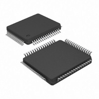
... Micrel, Inc. Package Information September 2010 103 KSZ8873MLL/FLL/RLL M9999-092309-1.2 ...
Page 104
... Purchaser’s use or sale of Micrel Products for use in life support appliances, devices or systems is a Purchaser’s own risk and Purchaser agrees to fully September 2010 Figure 32. 64-Pin LQFP Package indemnify Micrel for any damages resulting from such use or sale. © 2008 Micrel, Incorporated. 104 KSZ8873MLL/FLL/RLL M9999-092309-1.2 ...