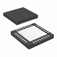
LM8333FLQ8X/NOPB National Semiconductor, LM8333FLQ8X/NOPB Datasheet

LM8333FLQ8X/NOPB
Specifications of LM8333FLQ8X/NOPB
Available stocks
Related parts for LM8333FLQ8X/NOPB
LM8333FLQ8X/NOPB Summary of contents
Page 1
... I/O, or host activity. 4.0 Block Diagram I2C ® registered trademark of Phillips Corporation. © 2010 National Semiconductor Corporation LM8333 The device is packaged in a 32–pin Leadless Leadframe package (LLP) and a 49-pin MICRO-ARRAY . Both are chip- scale packages. 2.0 Features ■ ...
Page 2
Ordering Information NSID Spec. LM8333FLQ8X NOPB* LM8333FLQ8Y NOPB LM8333GGR8 NOPB LM8333GGR8AXS** NOPB * NOPB = No PB (No Lead) ** Please refer to Section 9.5 HOST READ COMMANDS 6.0 Pin Assignments www.national.com No. of Pins Package Type Temperature 32 ...
Page 3
General Description ......................................................................................................................... 1 2.0 Features ........................................................................................................................................ 1 3.0 Applications .................................................................................................................................... 1 4.0 Block Diagram ................................................................................................................................ 1 5.0 Ordering Information ........................................................................................................................ 2 6.0 Pin Assignments ............................................................................................................................. 2 7.0 Signal Descriptions .......................................................................................................................... 4 8.0 Typical Application ........................................................................................................................... 5 8.1 FEATURES ...
Page 4
Signal Descriptions Name 32 Pins WAKE_IN0 29 WAKE_IN1 30 WAKE_IN2 27 WAKE_IN3 28 WAKE_IN4 31 WAKE_IN5 32 WAKE_IN6 1 WAKE_IN7 2 K_OUT0 21 K_OUT1 22 K_OUT2 23 K_OUT3 24 K_OUT4 3 K_OUT5 4 K_OUT6 5 K_OUT7 6 GEN_IO_0 12 ...
Page 5
Typical Application 8.1 FEATURES The following features are supported: • standard keys. • 8 special function keys (SF keys) with wake-up capability by forcing a WAKE_INx pin to ground. Pressing a SF key overrides any other ...
Page 6
The LM8333 will remain in Active mode as long as a key event, or any other event, which causes the IRQ output to be asserted is not resolved. 8.4.1 ACCESS.bus Activity When the LM8333 is in Halt mode, any activity ...
Page 7
Event Number Event Code 1 0xF1 2 0xB6 3 0x71 4 0x36 5 0xB4 6 0x34 7 0x91 8 0x00 FIGURE 2. Example Event Codes Loaded in FIFO Buffer 9.2 I/O EXPANSION In addition to keypad scanning, the LM8333 supports ...
Page 8
OUT_DIR Bit PWM_DIR Bit 9.2.2 General-Purpose I/O (GPIO) Figure 5 shows the commands to write, read and control the general-purpose I/O port pins, GEN_IO_0, GEN_IO_1, GEN_IO_2, and GEN_IO_3. Table 4 shows the pin configuration for all ...
Page 9
TABLE 5. Interface Commands for Controlling the LM8333 Function Cmd Dir R FIFO_READ 0x20 RPT_FIFO_READ 0x21 R W DEBOUNCE 0x22 GEN_IO_IN 0x30 R GEN_IO_OUT 0x31 W W GEN_IO_DIR 0x32 PWM_HI 0x40 W PWM_LO 0x41 W W PWM_CTL 0x42 READ_INT 0xD0 ...
Page 10
Every transfer is preceded by a Start condition ( Re- peated Start condition (RS). The latter occurs when a com- mand follows immediately upon another command without an intervening Stop condition (P). A Stop condition indicates the end ...
Page 11
WAKE-UP FROM HALT MODE Any bus transaction initiated by the host may encounter the LM8333 device in Halt mode or busy with processing data, such as controlling the FIFO buffer or executing interrupt ser- vice routines. Figure 10 shows ...
Page 12
Interrupts 10.1 INTERRUPT CODE The interrupt code is read and acknowledged with the READ_INT command (0xD0). This command clears the code and deasserts the IRQ output. Table 6 the interrupt code Bit Description ...
Page 13
FIGURE 11. Interrupt Processing 13 20210613 www.national.com ...
Page 14
COMMAND EXECUTION SUMMARY • With the interrupt, status, and error codes, the LM8333 provides the features needed to support a reliable key- scan functionality. • key-scan events can be stored in an internal FIFO buffer. The ...
Page 15
... Absolute Maximum Ratings 1) If Military/Aerospace specified devices are required, please contact the National Semiconductor Sales Office/ Distributors for availability and specifications. Supply Voltage ( Voltage at Any Pin Maximum Input Current Without Latchup 12.0 DC Electrical Characteristics ≤ ≤ (Temperature: -40°C TA +85°C) Data sheet specification limits are guaranteed by design, test, or statistical analysis ...
Page 16
AC Electrical Characteristics ≤ ≤ (Temperature: -40°C T +85°C) A Data sheet specification limits are guaranteed by design, test, or statistical analysis. Parameter Internal Oscillator System Oscillator (mclk) System Oscillator and Internal Frequency Variation Input Pulse Width Low Input ...
Page 17
17 www.national.com ...
Page 18
Physical Dimensions www.national.com inches (millimeters) unless otherwise noted Leadless Leadframe Package Order Number LM8333FLQ8X or LM8333FLQ8Y NS Package Number LQA32A Micro Array Package Order Number LM8333GGR8 or LM8333GGR8AXS NS Package Number GRA49A 18 ...
Page 19
Notes 19 www.national.com ...
Page 20
... For more National Semiconductor product information and proven design tools, visit the following Web sites at: www.national.com Products Amplifiers www.national.com/amplifiers Audio www.national.com/audio Clock and Timing www.national.com/timing Data Converters www.national.com/adc Interface www.national.com/interface LVDS www.national.com/lvds Power Management www.national.com/power Switching Regulators www.national.com/switchers LDOs www.national.com/ldo LED Lighting www ...


