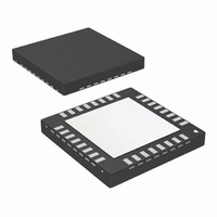
LM8333FLQ8X/NOPB National Semiconductor, LM8333FLQ8X/NOPB Datasheet - Page 8

LM8333FLQ8X/NOPB
Manufacturer Part Number
LM8333FLQ8X/NOPB
Description
IC KEYPAD CTLR 32-LLP
Manufacturer
National Semiconductor
Datasheet
1.LM8333GGR8NOPB.pdf
(20 pages)
Specifications of LM8333FLQ8X/NOPB
Controller Type
I/O Controller
Interface
ACCESS.bus, Microwire/SPI, USART, USB
Voltage - Supply
2.25 V ~ 2.9 V
Current - Supply
6mA
Operating Temperature
-40°C ~ 85°C
Mounting Type
Surface Mount
Package / Case
32-LLP
For Use With
LM8333EVALKIT - BOARD EVALUATION LM8333
Lead Free Status / RoHS Status
Lead free / RoHS Compliant
Other names
LM8333FLQ8X
Available stocks
Company
Part Number
Manufacturer
Quantity
Price
Company:
Part Number:
LM8333FLQ8X/NOPB
Manufacturer:
NS
Quantity:
3 808
Company:
Part Number:
LM8333FLQ8X/NOPB
Manufacturer:
TI/NS
Quantity:
9
www.national.com
9.2.2 General-Purpose I/O (GPIO)
Figure 5
general-purpose I/O port pins, GEN_IO_0, GEN_IO_1,
GEN_IO_2, and GEN_IO_3.
Table 4
of control bit settings (data output and direction) for the gen-
eral-purpose I/O pins. GEN_IO_3 cannot be put into the high
9.2.3 External Interrupts
When the GEN_IO_0 or GEN_IO_1 pins are configured as
inputs, a SET_EXT_INT command (0xD1) can be used to
enable receiving external interrupts on either or both of these
pins. Setting the EX_0 or EX_1 bits in the data byte of the
SET_EXT_INT command (as shown in
corresponding pin as an external interrupt input. When en-
abled as an interrupt input, any rising or falling edge causes
the IRQ output to be asserted. If the LM8333 was in Halt
mode, it also wakes up into Active mode.
OUT_DIR Bit
GEN_IO_DIR Bit
shows the pin configuration for all four combinations
shows the commands to write, read and control the
X
0
1
0
0
0
1
1
PWM_DIR Bit
FIGURE 5. General-Purpose I/O Control Commands
TABLE 4. General Purpose I/O Pin Configuration
Figure
X
1
1
0
TABLE 3. Summary of PWM Control Bits
GEN_IO_OUT Bit
6) enables the
0
1
0
1
MOD BIT
8
0
0
0
1
All general-purpose I/O pins can be programmed as inputs or
outputs as shown in
pins provide an additional capability for programmable wake-
up.
impedance (Hi-Z) input mode. When programmed as an in-
put, it can only be configured as an input with a weak pullup.
When both GEN_IO_0 and GEN_IO_1 are configured as in-
terrupt inputs, bits 1 and 2 of the interrupt code indicate which
input asserted the interrupt. However, if only one of
GEN_IO_0 or GEN_IO_1 is configured as an interrupt input,
both bits 1 and 2 of the interrupt code will be set when an
interrupt occurs.
FIGURE 6. SET_EXT_INT Command Data Byte
Direction
Output
Output
Input
Input
Drive output low
Drive output high
TRI-STATE® mode
PWM timer output
Table
4. The GEN_IO_0 and GEN_IO_1
Description
Weak Pullup
20210607
Drive High
Drive Low
State
Hi-Z
20210608


