L4938N STMicroelectronics, L4938N Datasheet - Page 7
L4938N
Manufacturer Part Number
L4938N
Description
Linear Regulators - Standard Dual 5V Very LDO
Manufacturer
STMicroelectronics
Datasheet
1.L4938N.pdf
(12 pages)
Specifications of L4938N
Polarity
Positive
Number Of Outputs
2
Output Type
Selectable
Output Voltage
5 V
Output Current
5 mA
Line Regulation
20 mV
Load Regulation
50 mV
Dropout Voltage (max)
0.4 V
Input Voltage Max
28 V
Maximum Operating Temperature
+ 150 C
Minimum Operating Temperature
- 55 C
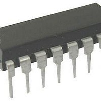
Package / Case
PDIP-16
Maximum Power Dissipation
875 mW
Mounting Style
Through Hole
Reference Voltage
1.23 V
Voltage Regulation Accuracy
2 %
Lead Free Status / Rohs Status
Lead free / RoHS Compliant
Available stocks
Company
Part Number
Manufacturer
Quantity
Price

Part Number:
L4938N
Manufacturer:
ST
Quantity:
20 000
Company:
Part Number:
L4938ND013TR
Manufacturer:
HITACHI
Quantity:
691
Company:
Part Number:
L4938NPD
Manufacturer:
ST
Quantity:
5 510


RESET CIRCUIT
The block circuit diagram of the reset circuit is shown
in fig. 4. The reset circuit supervises the standby out-
put voltage. The reset threshold of 4.7V is defined
by the internal reference voltage and the standby
output divider.
The reset pulse delay time t
charge time of an external capacitor C
The reaction time of the reset circuit depends on the
discharge time limitation of the reset capacitor C
and is proportional to the value of C
The reaction time of the reset circuit increases the
noise immunity. In fact, if the standby output voltage
drops below the reset threshold for a time shorter
than the reaction time t
Figure 4: Block Diagram of the Reset Circuit.
t
RD
=
C
RR
T
2 A
x 2V
, no reset output variation
RD
, is defined by the
T
.
T
:
T
occurs. The nominal reset delay is generated for
standby output voltage drops longer than the time
necessary for the complete discharging of the ca-
pacitor C
C
shown in fig. 5.
SENSE COMPARATOR
This circuit compares an input signal with an internal
voltage reference of typically 1.23V. The use of an
external voltage divider makes the comparator very
flexible in the application. This function can be used
to supervise the input voltage - either before or after
the protection diode - and to give additional informa-
tion to the microprocessor such as low voltage warn-
ings.
If this feature is not used SI and SO have to con-
nected to GND. In this case the St-by quiescent cur-
rent (14V) increases from 290 A to 300 A.
T
= 100nF. The typical reset output waveforms are
T
. This time is typically equal to 50 s if
L4938N - L4938ND - L4938NPD
7/12
Related parts for L4938N
Image
Part Number
Description
Manufacturer
Datasheet
Request
R

Part Number:
Description:
STMicroelectronics [RIPPLE-CARRY BINARY COUNTER/DIVIDERS]
Manufacturer:
STMicroelectronics
Datasheet:
Part Number:
Description:
STMicroelectronics [LIQUID-CRYSTAL DISPLAY DRIVERS]
Manufacturer:
STMicroelectronics
Datasheet:

Part Number:
Description:
BOARD EVAL FOR MEMS SENSORS
Manufacturer:
STMicroelectronics
Datasheet:
Part Number:
Description:
NPN TRANSISTOR POWER MODULE
Manufacturer:
STMicroelectronics
Datasheet:
Part Number:
Description:
TURBOSWITCH ULTRA-FAST HIGH VOLTAGE DIODE
Manufacturer:
STMicroelectronics
Datasheet:
Part Number:
Description:
Manufacturer:
STMicroelectronics
Datasheet:
Part Number:
Description:
DIODE / SCR MODULE
Manufacturer:
STMicroelectronics
Datasheet:
Part Number:
Description:
DIODE / SCR MODULE
Manufacturer:
STMicroelectronics
Datasheet:
Part Number:
Description:
Search -----> STE16N100
Manufacturer:
STMicroelectronics
Datasheet:
Part Number:
Description:
Search ---> STE53NA50
Manufacturer:
STMicroelectronics
Datasheet:
Part Number:
Description:
NPN Transistor Power Module
Manufacturer:
STMicroelectronics
Datasheet: